
INDUSTRY ANALYSIS
Why AI Is Driving More Testing: From HBM Probe Cards to CPO Optoelectronic Test
As AI chips move toward higher power, multiple dies, and advanced packaging, testing demand is being driven by shipment volumes, test complexity, and the cost of failure. HBM reinforces the need to screen for known good dies before packaging, while CPO adds precision optical coupling, coordinated optical/electrical measurement, and automation challenges. This article examines these two growth paths and reviews public progress at FormFactor, MPI, WinWay, CHPT, Enlitech, and Chroma.
When discussing AI hardware, the market tends to focus on GPUs, HBM, advanced packaging, and cooling. Before these components become products that can ship reliably, they must also pass another stage: testing.
As a package integrates more dies, memory, and high-speed interfaces, the cost of overlooking one defective die rises. Manufacturers need to establish component quality earlier and verify after assembly that the parts work together. AI therefore raises both the technical demands of testing and its importance to product cost and yield management.[1][2]
Understanding this demand requires separating three questions: why test workloads are growing, what additional work HBM and CPO each create, and which suppliers have already converted technical capabilities into orders or revenue.
How AI Increases Test Workloads
More Expensive Chips and Packages Make Early Screening More Valuable
Advanced packaging integrates compute dies, memory, interposers, and other components. If a problem is discovered only after expensive assembly is complete, losses may include other good components as well as the processing costs already incurred.
Customers therefore place greater emphasis on known good die (KGD): bare dies screened through specified tests before downstream assembly. KGD is not a guarantee that a chip will never fail. Appropriate test coverage reduces the likelihood of defective parts entering costly processes.[1]
This also explains customers’ willingness to use more capable, potentially more expensive probe cards. Evaluation considers not only cost per test but also the downstream losses that testing can prevent.
Multidie Architectures Add Verification Before and After Assembly
Chiplet and multidie packages divide functions among several dies and integrate them through advanced packaging. Even after individual dies pass testing, assembly can introduce bonding, interconnect, and thermal-management problems, creating a need for verification at different process stages.
Demand does not grow only at the final shipment test. Testing can move upstream to wafers, individual dies, or intermediate assembly stages so that manufacturers identify problems earlier. Teradyne’s analysis of AI chiplets identifies new test insertions, power delivery, cooling, and contact methods as important changes associated with advanced packaging.[2]
Product flows differ, and not every chip gains the same number of test stages. Nevertheless, final chip shipments alone are no longer enough to assess equipment loading.
High Speed and High Power Make Test Interfaces More Demanding
High-speed signals, large currents, and dense contacts require AI probe cards and test sockets to address both mechanical contact and electrical performance.
Probes must make consistent contact in limited space. Test interfaces need to control signal loss, crosstalk, and power-supply voltage drops. High-power testing must also prevent chip overheating and damage to probe cards and sockets. Teradyne’s AI test instruments introduced in 2026 emphasize larger test-vector memory, high-speed interfaces, and power-fault protection.[3]
A high-end probe card’s value therefore cannot be judged simply by its number of probes. Customers are buying the ability to obtain trustworthy results repeatedly at specified temperatures, currents, and signal speeds.
System-Level Test Places More Emphasis on Real Operating Conditions
Some problems are more readily exposed when a chip runs workloads resembling actual applications. System-level test, or SLT, is an important way to address these verification needs.
SLT can check stability when multiple functions operate together, alongside power delivery and active temperature control. Teradyne’s Titan HP is already used in production testing by several customers, and its design reflects the power, thermal, and throughput demands of AI and cloud chips.[4]
SLT, conventional functional testing, and burn-in serve different purposes; they should not all be described as simply “testing for longer.”
Equipment demand depends on the number of units under test, test time at each stage, parallel test capacity, and actual available operating time. Even with unchanged chip shipments, additional test content can increase equipment loading. Conversely, parallel testing, process improvements, and automation can offset some of that increase. Test-business growth cannot simply be extrapolated in proportion to AI chip shipments.[4][5]
Why HBM Drives High-End Probe Cards
HBM integrates multiple DRAM layers and associated base dies into a stacked structure for high-bandwidth computing systems. A key testing objective is to verify each die as thoroughly as practical before stacking, keeping defective dies out of subsequent processes.
A typical flow can include wafer-stage screening, post-stack checks according to the manufacturing process, and verification after packaging. Screening for known good dies before stacking and checking interconnects afterward address different problems.[6]
These requirements make probe cards balance fine-pitch contact, high-speed electrical performance, power delivery, and parallel test efficiency. A probe card is the precision connection between test equipment and the chip under test; it is not itself the tester that performs all pass/fail evaluation.[1][7]
For suppliers, HBM opportunities include greater wafer-test volumes, upgraded test specifications, and probe-card requirements for different product designs. Actual purchasing still depends on test flows, sharing across products, service life, and customers’ capacity allocation.
FormFactor provides a clear commercialization example: in its Q2 2025 results announcement, it said it was shipping in volume to all three major HBM manufacturers. This is public evidence of HBM testing demand translating into probe-card orders.[8]
What Different Probing Requirements Does CPO Add?
Co-packaged optics, or CPO, places optical engines closer to switching or compute-related chips within a packaging architecture, shortening some high-speed electrical paths. It retains electronic circuits while adding optical paths and electrical/optical conversion, so testing must cover both.
Optical testing already exists in the communications industry. CPO’s new challenge is incorporating it into denser wafer, die, and package integration flows at the speed, repeatability, and cost needed for production.[9][10]
| Test dimension | What needs to be established | Additional equipment requirements |
|---|---|---|
| Electrical contact and measurement | Whether power, control signals, and high-speed electrical interfaces function correctly | High-frequency/high-speed probes, sockets, power delivery, and measurement instruments |
| Optical coupling and path measurement | Whether light can consistently enter and leave the chip and whether losses meet requirements | Fiber probing interfaces, precision alignment, calibration, and optical measurement |
| Coordinated optical/electrical verification | Whether data quality is acceptable after electrical-to-optical conversion and reception | Synchronized electrical/optical measurements, with eye diagrams, bit-error rate, or receiver sensitivity measured as appropriate to the stage |
| Temperature and production repeatability | Whether consistent results persist across dies and temperature changes | Temperature control, handling, automatic alignment, software workflows, and equipment integration |
These are requirements at different levels, not a claim that every test insertion performs every item.[9][10]
Optical alignment is substantial work beyond electrical testing. Electrical probes must consistently contact pads, while fibers or optical probing interfaces must align with the chip’s optical coupling structures. Positional error can change coupling efficiency, making results depend on both chip performance and the test setup.[10]
This creates two production problems. Equipment must first distinguish loss originating in the chip from loss caused by alignment or coupling conditions. Second, precision alignment cannot take too long; a system can measure accurately yet still fail to meet production cycle times.
Competitive CPO testing therefore integrates optoelectronic measurement, mechanical positioning, automation, temperature control, and data management. Successfully measuring one chip during engineering and continuously testing many products on a production line are different capability thresholds.[9][10]
Why HBM Often Drives Probe Cards While CPO Also Drives Systems
The difference becomes clearer by examining what customers purchase.
HBM wafer testing needs high-performance probe cards that let existing test architectures contact and verify more advanced memory. CPO may require optical instruments, fiber alignment, electrical testing, wafer handling, and control software to be integrated into a test cell, creating demand for complete equipment and systems as well.
TRITON, developed through FormFactor’s collaboration with Advantest and Tokyo Electron, is an example of integrated wafer-level optical/electrical testing. It supports automated measurements and combines an electrical tester, probe cards, and optical coupling interfaces.[11]
The distinction has also appeared in financial disclosures. FormFactor’s Q2 2026 filing said HBM demand drove growth in DRAM probe-card revenue, while year-over-year growth in its Systems business came primarily from TRITON sales.[12]
This is not a fixed industry boundary: HBM also needs testers, handling, and temperature-control equipment, while CPO uses electrical probes, probe cards, and sockets. A supplier’s actual business should be identified by whether it delivers an interface, an instrument, integrated equipment, or testing services.
What Stage Have Taiwanese Suppliers Reached?
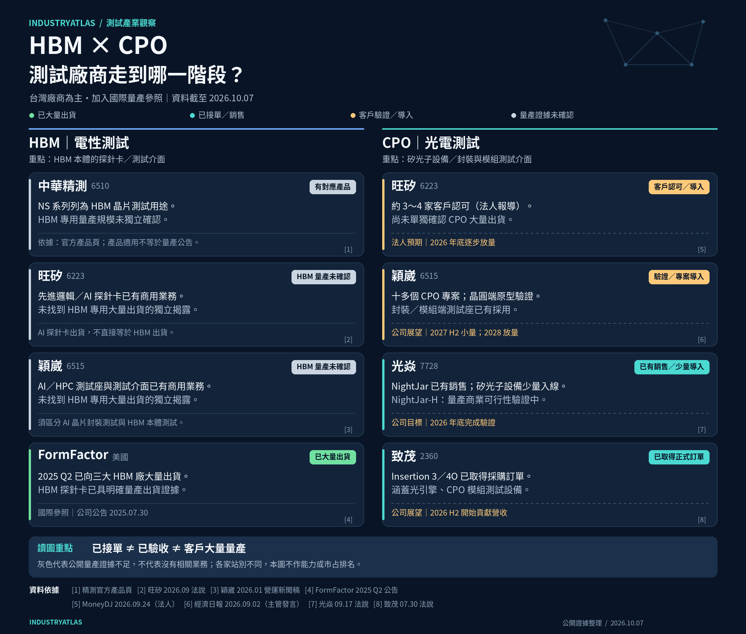
As of October 7, 2026, Taiwanese suppliers had reached different stages, including product applications, customer qualification, limited adoption, and confirmed orders. The table separates established developments from future expectations.
| Supplier | Relevant products and role | Confirmed public progress | Subsequent milestones |
|---|---|---|---|
| MPI (6223) | Probe cards and CPO/silicon-photonics test equipment | September 2026 reporting cited institutional analysts saying CPO equipment had received approval from about three to four customers | Analysts expected volumes to increase gradually from late 2026; subsequent shipments and revenue still need to confirm this.[13] |
| WinWay Technology (6515) | Wafer-level test interfaces and package/module test sockets | A company executive said in September that more than ten CPO projects were underway; wafer-level prototypes remained in customer qualification, while package/module solutions had already been adopted | Company outlook: small-volume shipments in the second half of 2027 and a further ramp in 2028.[14] |
| Enlitech (7728) | Silicon-photonics optical inspection, defect analysis, and high-throughput inspection platforms | NightJar had recorded sales; silicon-photonics equipment had entered R&D and engineering validation, with limited placement on customer production lines | NightJar-H remained in commercial-feasibility validation for high-volume manufacturing; the company targeted completion by the end of 2026.[15] |
| Chroma ATE (2360) | Optical-engine and CPO-module test equipment | Its July 2026 investor conference confirmed purchase orders for Insertion 3 and Insertion 4O, with a larger order scale than three months earlier | At the time, the company expected revenue contributions to begin in the second half of 2026; track delivery, acceptance, and follow-on orders.[16] |
| Chunghwa Precision Test Tech. / CHPT (6510) | Probe cards and test interfaces | Its official product page lists the NS series as suitable for HBM chip testing | The application scope is disclosed, but the scale of HBM-specific volume production has not been independently established.[17] |
Separate MPI and WinWay’s Existing AI Businesses From Their New Products
MPI has an established probe-card business, and WinWay already serves AI and high-performance-computing test interfaces. Growth in those existing businesses cannot be treated as direct evidence that HBM-specific probe cards or CPO test equipment are already shipping in large volumes.[18][19]
“Testing an AI chip package containing HBM” also differs from “directly testing HBM memory.” Both may belong to the same AI supply chain, but the devices under test and product requirements are different.
WinWay’s CPO progress likewise shows that prototype validation, adoption of interfaces, and a future volume ramp can coexist. Some solutions entering customer projects does not mean all test insertions have completed production deployment.[14]
Enlitech’s Existing Sales and Production-Version Validation Are Separate Milestones
Enlitech’s NightJar has an established sales record, while the higher-throughput NightJar-H remains in validation of commercial feasibility for high-volume manufacturing.
The established progress is therefore entry into R&D, engineering validation, and limited production-line applications. The next question is whether completed validation leads to sustained purchases of production equipment.
The company presentation’s CIS image-sensor inspection business, explicitly described as being on customer mass-production lines, should also be interpreted separately from the validation status of its silicon-photonics products.[15]
Chroma’s CPO Portfolio Already Covers Optical-Engine and Module Testing
Chroma’s relevant business includes reliability testing as well as the 58721 optical-engine optoelectronic test system and the 58711 CPO switch-module test system. Product information and confirmed orders show that the company is participating in commercial deployment of CPO optoelectronic test equipment.[16][20]
An “insertion” is a test stage within a manufacturing process. Suppliers and customers may subdivide or number these stages differently. The insertion number should therefore be considered alongside the object under test—such as an optical engine, module, or wafer—rather than compared on its own.
For Chroma, the next issue is how orders turn into equipment delivery, acceptance, and recurring revenue. Receiving purchase orders and a broad production ramp of end-market CPO products remain different events.
What Evidence Should Be Tracked to Assess Testing Opportunities?
Three transitions are useful to follow in sequence:
1. From technical demonstration to customer adoption. Has the product entered an actual qualification process, and does it meet the customer’s speed, accuracy, and stability requirements? 2. From purchase orders to delivery and revenue. Have ordered systems passed acceptance, and does revenue come from R&D equipment, engineering tools, or production equipment? 3. From initial adoption to sustained expansion. Does the same customer reorder, and can the supplier expand across customers, product generations, or test insertions?
The value of testing in the AI era comes from helping manufacturers consistently turn complex chips into qualified products at an acceptable cost. HBM makes electrical screening before packaging more important, while CPO brings precision optical alignment and coordinated optoelectronic verification into production flows.
For test suppliers, rising technical difficulty creates opportunities to upgrade products. Sustained benefits still depend on customer qualification, production efficiency, delivery capabilities, and actual purchasing. Keeping “the product can do it,” “customers have started buying,” and “volume production continues to expand” separate is essential to understanding each supplier’s real position.
Sources & notes
- Sources primarily comprise company product information, investor presentations, and filings. Institutional analysts’ forecasts and executives’ public outlooks are identified in the text and are not treated as achieved production milestones.
- 1. FormFactor: From Commodity to Enabler — Wafer Test at the Heart of the AI Era
- 2. Teradyne: AI Chiplet Architectures Redefining Test Insertions — July 27, 2026
- 3. Teradyne: UltraFLEXplus instruments for AI and data-center testing — September 2026
- 4. Teradyne: Titan HP system-level test platform
- 5. Advantest: 7038 high-parallelism SLT and burn-in platform
- 6. FormFactor: High-Bandwidth Memory Testing — Why Early Test Strategies Are Critical for Yield, Cost, and Performance
- 7. FormFactor: HBM and memory wafer-test applications
- 8. FormFactor: Q2 2025 results — July 30, 2025
- 9. Quantifi Photonics: Scaling Photonics Test for PICs and Co-Packaged Optics
- 10. FormFactor: Six Challenges in Silicon Photonics Testing and Modern Engineering Solutions — July 30, 2026
- 11. FormFactor: TRITON silicon-photonics volume-production test system
- 12. FormFactor: Q2 2026 Form 10-Q, revenue discussion on page 26
- 13. MoneyDJ: MPI expected to set successive quarterly highs in the second half and strengthen next year — September 24, 2026; CPO timing reflects institutional analysts’ views
- 14. Economic Daily News: WinWay CPO test-socket progress and executive comments — September 2, 2026
- 15. Enlitech: Investor presentation, September 17, 2026, pages 8 and 23
- 16. Chroma: Q2 investor-conference transcript, July 30, 2026 — Quartr / Stock Analysis
- 17. CHPT: Official market applications and HBM probe-card information
- 18. MPI: September 2026 investor presentation
- 19. WinWay: January 2026 business update
- 20. Chroma: Q2 investor presentation, July 30, 2026, CPO test-product pages