
INDUSTRY ANALYSIS
How CPO Addresses High-Speed Interconnect Bottlenecks: Seven Manufacturing Stages and the Challenges of Scaling Production
CPO moves optical engines next to the switch ASIC, shortening high-speed electrical paths and opening up new possibilities for bandwidth density and energy efficiency. That integration also makes cooling, precision alignment, yield, and repair more challenging. This article follows seven stages—lasers, PICs/EICs, optical engines, fiber connections, packaging, testing, and complete systems—to explain the engineering problems at each stage and the roles of participating suppliers.
Why do AI data centers need CPO?
As AI systems grow, the amount of data exchanged between chips continues to increase. The challenge for high-speed interconnects is expanding from “Can we transmit faster?” to “Can we keep increasing throughput within limited power, cooling, and space budgets?”
Co-packaged optics (CPO) places optical engines in a shared package with a switch ASIC or another main chip, converting data from electrical to optical signals earlier in the path. The key is to shorten the distance traveled by high-speed electrical signals. This reduces transmission losses and the burden of signal compensation, improving interconnect power consumption and bandwidth density. [1]
The change also raises the difficulty of integration. Once optical components sit close to high-power chips, fabrication, thermal management, fiber alignment, yield, and repair must be considered together. CPO's industrial value is consequently spread across the supply chain.
The technical advance: converting data to light earlier
Conventional pluggable optical modules already use fiber, but the conversion between electrical and optical signals usually takes place near the equipment's front panel. Data leaving the switch ASIC must first pass through the package, PCB traces, and connectors before reaching the optical module.
Conventional architecture: switch ASIC → longer board-level electrical path → pluggable optical module → fiber.
CPO architecture: switch ASIC → short electrical connection within the package → optical engine → fiber.
As the per-lane data rate rises, attenuation, reflections, and crosstalk become harder to control. Drivers, equalization, and receiver circuits compensate to maintain signal quality, but they also consume power. By shortening the electrical path, CPO reduces the compensation required and concentrates more high-speed channels within a limited package footprint. [1]
CPO should therefore be evaluated in terms of power per unit of throughput and the bandwidth available within a given space. How far signal processing, retiming, and error correction can be simplified still depends on the interfaces and the design of the complete link. [2]
What problems do the seven stages address?
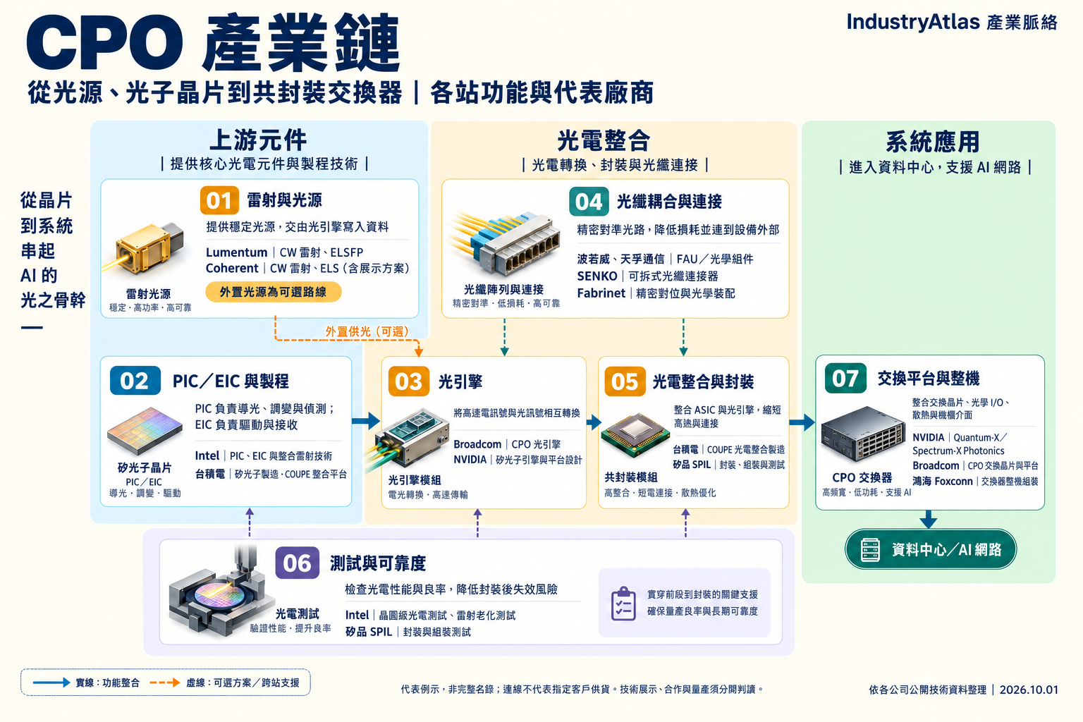
The following discussion focuses on CPO based on silicon photonics. These seven stages describe a division of functions. In actual manufacturing, some operations run in parallel, while testing spans several stages. A supplier may also participate in more than one stage.
| Stage | Main function | Core challenge | Improvement path |
|---|---|---|---|
| 01 Lasers and light sources | Provide stable optical power | Balancing temperature, power, and lifetime | Light-source placement, thermal management, and burn-in screening |
| 02 PICs/EICs and fabrication | Manufacture photonic and electronic components | Process differences, thermal sensitivity, and parasitics | Process control, heterogeneous integration, and temperature regulation |
| 03 Optical engines | Perform high-speed electrical/optical conversion | Interdependent electrical, optical, and thermal requirements | Co-design and link optimization |
| 04 Fiber coupling and connections | Guide light accurately into and out of the chip | Alignment losses and assembly consistency | Precision alignment, automation, and connector design |
| 05 Photonic/electronic integration and packaging | Integrate the ASIC and optical engines | High-density cooling, yield, and rework | Thermal-path planning and staged integration |
| 06 Testing and reliability | Screen defects and verify stable operation | Test coverage, time, and cost | Wafer-level testing, known-good-component screening, and traceability |
| 07 Switching platforms and complete systems | Deliver equipment that can operate in the field | System power, routing, and maintenance | System validation, monitoring, and serviceability design |
01 — Lasers and light sources: a stable supply of light over a long operating life
This stage provides the light needed by the optical engine. After splitting, modulation, coupling, and connection losses, enough laser power must still reach the receiver. Light-source specifications must therefore be designed around the losses of the entire link.
The difficulty is that increasing laser power also increases electricity consumption and heat. High temperatures can affect wavelength stability and operating life. When the light source is close to a high-power ASIC, reliability becomes a major design constraint.
One common approach is an external laser source (ELS): place the laser where temperature is easier to control and replacement is easier, then deliver light to the optical engine through fiber. Lumentum's related solutions address thermal paths, power and temperature margins, burn-in screening, and accelerated life testing to reduce the risk of failure. [3]
External light sources also add supply fibers and connections that need to be managed. Another approach integrates the light source, as in Intel's optical I/O technology. The trade-offs include integration density, optical loss, thermal management, and serviceability. [4]
02 — PICs/EICs and fabrication: making photonics and electronics work together
A photonic integrated circuit (PIC) guides, modulates, and detects light. An electronic integrated circuit (EIC) handles driving, reception, and associated control. Together, they form the foundation of high-speed electrical/optical conversion.
The challenge is that optical and electronic components have different requirements for materials, fabrication processes, and dimensions. Small variations in optical structures can change transmission characteristics. Connections between the two chips can also introduce parasitics that affect high-speed performance.
Heterogeneous integration allows each component to use a suitable fabrication process, then combines them through precision interconnects. TSMC's COUPE uses SoIC-X technology to stack the EIC on the PIC, shortening their electrical connections to improve electrical performance and efficiency. [5]
Some high-density designs use microring modulators. These are compact but sensitive to fabrication and temperature variations, requiring precise process control and temperature regulation. NVIDIA and TSMC's public collaboration materials identify microring manufacturing consistency and thermal sensitivity as engineering priorities. [6]
The production benchmark at this stage is whether fabricated components can meet specifications consistently and reliably.
03 — Optical engines: turning component specifications into usable transmission capacity
An optical engine integrates photonic components, electronics, and the necessary interfaces. During transmission, electronic circuits drive modulators to encode data onto light. During reception, photodetectors convert light into electrical signals, which are then processed by the receiver circuits.
Individually qualified components do not necessarily meet system targets once assembled. Drive requirements, optical loss, receiver sensitivity, noise, and cooling affect one another. For example, a design that reduces driver power but increases optical loss may require a more powerful light source, canceling out the original energy savings.
The solution is to co-design electrical circuits, optical paths, and thermal paths, assessing the benefit across the complete link. TSMC's COUPE platform addresses both EIC/PIC electrical connections and optical coupling loss while considering the requirements of co-packaging with the main chip. [7]
Optical engines and platforms from Broadcom, NVIDIA, and others can be understood in the same way: the objective is to maintain sufficient signal quality, power margin, and thermal margin while many channels operate at high speed simultaneously. [1][6]
04 — Fiber coupling and connections: making precise alignment repeatable
Once the optical engine is complete, its on-chip optical paths must connect to external fibers. A fiber array unit (FAU) positions multiple fibers at specified locations and spacing so that they align with the chip's optical interface.
Misalignment increases coupling loss. Multichannel designs must also maintain consistency across the entire fiber array. This stage must turn precise optical alignment into a manufacturing process that can be repeated at scale. [8]
Engineers can use active alignment, adjusting position while measuring an optical signal, or rely on precision structures and passive alignment to reduce the amount of individual adjustment. Fabrinet's disclosed optical communications manufacturing capabilities include active and passive alignment and precision assembly. Browave's product portfolio includes FAUs, fiber bundles, and related CPO components. [9][10]
Connector design further affects assembly and maintenance. SENKO's detachable optical connection solutions provide greater flexibility, while still needing to maintain low loss and performance through repeated connections. [11]
Reducing coupling loss gives both the upstream light source and the downstream receiver more design margin.
05 — Photonic/electronic integration and packaging: combining density with effective cooling
This stage integrates the ASIC and optical engines into a shared package, establishing short, high-density electrical connections that deliver CPO's architectural advantage.
Thermal management becomes more important as optical engines move closer to high-power chips. The package must accommodate electrical routing, fiber exits, cooling structures, and assembly access. Thermal paths, thermal isolation, and temperature monitoring must be planned together with the cooling design of the complete system. [2]
Package integration also affects cost. Once an expensive ASIC and multiple optical engines are combined into a module, a failure in any part can increase rework or scrap losses. Upstream screening for good components, staged testing, and feasible rework strategies must therefore be part of process planning.
TSMC provides photonic/electronic integration and manufacturing platforms, while assembly and test companies carry out packaging and validation work. For example, NVIDIA's disclosed manufacturing responsibilities for Spectrum-X Photonics identify SPIL as responsible for packaging, assembly, and testing. [12]
06 — Testing and reliability: finding defects before more cost accumulates
CPO testing must cover wafers, bare dies, optical engines, and complete packages to avoid building defective components into progressively more expensive products.
One important practice is to identify known-good dies before further integration. Intel's disclosed silicon photonics manufacturing capabilities include wafer-level electrical/optical testing and laser burn-in screening, improving confidence in the components sent to downstream assembly. [4]
Testing must extend beyond “Can it transmit data?” to “Under what conditions can it continue transmitting reliably?” Optical power, coupling loss, receiver capability, bit-error performance, and temperature variations all affect reliable operation. Results with many channels operating simultaneously are also more representative of real use than the best result from a single channel.
More comprehensive testing usually requires more time and equipment. This stage must therefore improve automation, test interfaces, and data traceability so that defects can be located and fed back to upstream processes. Test efficiency directly affects yield and the cost of each qualified product.
07 — Switching platforms and complete systems: equipment that can be deployed, monitored, and repaired
System-level evaluation must include the switch ASIC, optical engines, light sources, power supplies, and cooling. Power savings in an individual circuit become a real data center benefit only if they are preserved at the level of the complete system.
System manufacturers must also address fiber routing, access to connectors, fault diagnosis, and replacement procedures. External lasers, for example, can be designed for field replacement, while optical-engine repair still depends on the package architecture. NVIDIA's disclosed designs include socketed and soldered integration, each with different assembly and maintenance considerations. [6]
Platform suppliers such as NVIDIA and Broadcom define switching and optical interconnect architectures. System manufacturers combine the parts into equipment. NVIDIA's disclosed manufacturing process assigns system assembly to Foxconn, followed by system validation. [12]
The final question is whether, under real workloads, the complete equipment can continuously deliver sufficient bandwidth while keeping power consumption, failures, and repair time within acceptable limits.
What progress should observers track across the CPO supply chain?
The engineering responsibilities above suggest three levels of industry analysis.
First, system-level benefits. Power comparisons should establish whether light sources, signal processing, and cooling are included, and whether effective throughput and operating conditions are comparable. The energy savings of a component cannot be treated as the savings of the entire system.
Second, production capability. Beyond a one-off high-speed demonstration, assess multichannel consistency, process yield, test efficiency, and assembly cost. Consistent delivery of qualified products shows that engineering results are becoming scalable manufacturing capabilities.
Third, operation and maintenance. How a failed laser or optical engine is located, which parts can be replaced, and how many connections a replacement disrupts all affect the value of deployment.
By shortening electrical paths, CPO opens new design possibilities for high-speed interconnects. The seven stages collectively determine how much of that advantage survives in practice. As light-source stability, precision assembly, packaging yield, and maintenance efficiency keep pace with bandwidth, CPO can continue expanding into real applications.
This article organizes functional responsibilities using suppliers' public technical materials. Architectures, supplier combinations, and adoption stages differ across platforms. The companies cited are examples, not a complete supplier list for any single product.
Sources & notes
- References [1]–[12] correspond to the citations in the text.
- [1] Broadcom: CPO architecture and high-speed electrical interconnect bottlenecks.
- https://www.broadcom.com/info/optics/cpo
- [2] OIF: Co-Packaging Framework Document; interfaces, thermal management, reliability, and serviceability.
- https://www.oiforum.com/wp-content/uploads/OIF-Co-Packaging-FD-01.0.pdf
- [3] Lumentum: White paper on external laser source reliability.
- https://www.lumentum.com/sites/default/files/2026-06/elsfpreliability-wp-cl-ae.pdf
- [4] Intel: Silicon photonics, integrated light sources, wafer-level testing, and laser burn-in screening.
- https://www.intel.com/content/www/us/en/products/details/network-io/silicon-photonics.html
- [5] TSMC: COUPE and SoIC-X integration technology. This article cites the architecture; it does not infer current production status from the plans announced at that time.
- https://pr.tsmc.com/english/news/3136
- [6] NVIDIA: Microring modulators, optical engines, and package integration approaches.
- https://developer.nvidia.com/blog/how-industry-collaboration-fosters-nvidia-co-packaged-optics/
- [7] TSMC: Research on COUPE photonic/electronic heterogeneous integration.
- https://research.tsmc.com/page/interconnect/30.html
- [8] Corning: CPO and the principles of fiber coupling.
- https://www.corning.com/optical-communications/emea/en/home/the-signal-network-blog/what-is-co-packaged-optics.html
- [9] Fabrinet: Precision assembly and active/passive alignment capabilities for optical communications.
- https://fabrinet.com/markets/opticalcommunications
- [10] Browave: CPO and optical component portfolio in its 2025 investor presentation. A product portfolio does not establish volume supply to a specific platform.
- https://www.browave.com/uploads/images/Investors%20Conference%20Call%202025.pdf
- [11] SENKO: NVIDIA photonics ecosystem and detachable optical connection solutions.
- https://www.senko.com/senko-advanced-components-joins-nvidia-photonics-ecosystem/
- [12] NVIDIA: Spectrum-X Photonics manufacturing responsibilities disclosed at Computex 2026.
- https://blogs.nvidia.com/blog/nvidia-gtc-taipei-computex-2026-news/