
INDUSTRY ANALYSIS
Innolux Enters RDL and Advanced Packaging: Large-Area Manufacturing Advantages, Production Hurdles, and Competitive Implications
As AI chips integrate more compute dies and memory into a single package, the industry’s challenge is expanding from making transistors smaller to connecting more chips while controlling packaging costs. This is the backdrop to Innolux’s move into RDL and advanced packaging. Its experience in large-area processing, thin-film patterning, and automation provides a starting point. The opportunity lies in turning those capabilities into routing substrates and packaging services that customers can use, then using a larger manufacturing area to lower the cost per good package. Area alone is only one factor: fine traces, multilayer interconnects, warpage control, package reliability, and consistent delivery will determine how far this transition can go.
What Innolux Is Building: RDL Substrates and Complete Packaging Are Different Businesses
Innolux’s publicly disclosed packaging portfolio includes chip-first and RDL-first packaging, RDL substrates, glass-core substrates, and panel-level testing services.[1]
These businesses can connect with one another, but they occupy different positions in the supply chain. If Innolux supplies an RDL substrate with completed routing, its downstream customer can still handle die attachment, packaging, and testing. If Innolux takes on the complete package, it must also handle chip interconnection, assembly, and final quality. The former can make it a supplier to existing packaging companies; the latter puts it more directly into the outsourced packaging market.
Two public disclosures are particularly important to distinguish:
| Item | Innolux’s public disclosure | How to interpret it at this stage |
|---|---|---|
| RDL substrate | 620 × 750 mm; uses existing G3.5 lines with added panel-level electroplating; supports fine-pitch copper traces and multilayer routing; can be cut into 18 strips for downstream processing | A product and manufacturing approach have been disclosed. The exhibitor information does not provide comparable minimum line/space, an exact layer count, or production yield. |
| Chip-last / HIPoS platform | 620 × 670 mm; minimum line/space of 2/2 μm; combines multilayer RDL with an embedded core structure for AI/HPC | Development results were announced in September 2026, with customer qualification to follow and mass production targeted for the second half of 2027. |
Sources: Innolux’s official SEMICON Taiwan 2026 exhibitor information and company press release.[1][2]
These dimensions come from different product disclosures. The 620 × 750 mm format, 2/2 μm line/space, multilayer capability, and mass-production target must not be combined into one supposedly qualified specification. Innolux also says its existing chip-first panel testing solution has a production track record, but that does not establish that its new chip-last platform has reached the same stage.[2]
What Is RDL, and Why Might a Display Manufacturer Have an Opening?
RDL stands for redistribution layer. Made from metal traces and insulating materials, it rearranges the positions of a chip’s connection points and can also connect chips within a multichip package.
A chip’s pads may be densely spaced or poorly positioned for direct connection to a package substrate or circuit board. RDL routes those connections outward and redistributes them to suit the package. In packages containing multiple dies, it can also form a lateral interconnect network.
RDL has long been used in semiconductor packaging. Amkor’s wafer bumping services, for example, already offer single- and multilayer redistribution with volume-production capabilities for 200 mm and 300 mm wafers.[3] RDL therefore did not originate with Innolux’s entry, the emergence of FOPLP, or glass substrates.
Understanding Innolux’s opportunity requires separating three concepts:
- RDL is a routing structure and process. The focus is how pads connect through metal traces and interlayer vias. - FOPLP means fan-out panel-level packaging. The focus is using a rectangular panel for batch manufacturing, with package routing extending beyond the die footprint. - A glass-core substrate is a material and structural choice. Whether glass remains in the final product is a different question from whether it serves only as a temporary processing carrier.
Panel-level packaging can use RDL, but RDL is not limited to panel-level packaging. Likewise, fabricating RDL on a glass carrier does not mean the final product necessarily retains a glass core. Vertical connections through glass introduce another topic: through-glass vias, or TGVs.
How RDL Is Made: Building Up Metal Traces and Insulating Layers
RDL can be understood as a miniature multilayer circuit. Horizontal copper traces carry signals to different positions; vertical vias connect layers; dielectric materials isolate conductors that should not be electrically connected.
The following is a typical RDL buildup cycle using the semi-additive process (SAP). It illustrates a general industry process, not an undisclosed proprietary Innolux recipe. The first-layer and downstream sequences can differ by package architecture.[4][5]
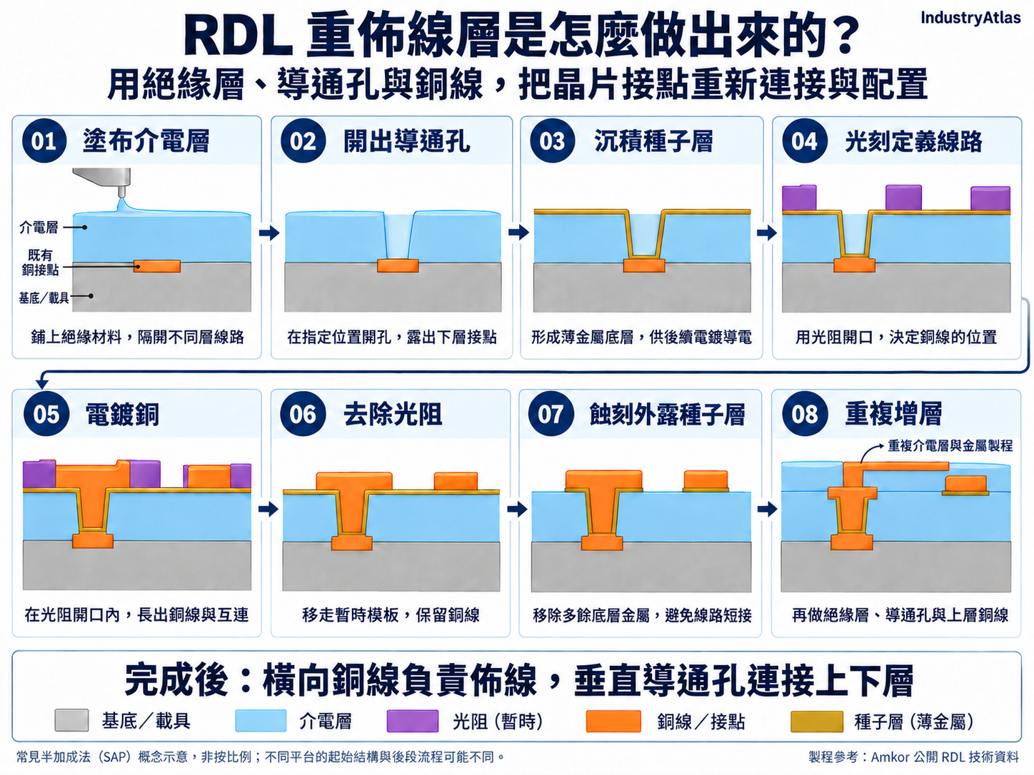
| Step | What the process does |
|---|---|
| 1. Prepare the processing surface | Establish a workable surface using a carrier or a reconstituted die/mold structure. |
| 2. Form the dielectric layer | Coat and cure an insulating material to separate metal traces on different layers. |
| 3. Create vias | Use exposure and development, or a combination with etching, to open the dielectric and expose the pads to be connected. |
| 4. Deposit a metal seed layer | Form a thin conductive base that enables subsequent electroplating and continuous metal formation. |
| 5. Define the circuit by lithography | Pattern openings in photoresist to define the positions and shapes of copper traces. |
| 6. Electroplate copper | Build up copper in the openings to form traces and interlayer connections. |
| 7. Strip resist and etch the seed layer | Remove the temporary photoresist and exposed base metal to electrically isolate the traces. |
| 8. Repeat buildup and inspect | Add further dielectric layers, vias, and copper traces to complete the interconnect structure layer by layer. |
After RDL formation, the package architecture may still require bumps or solder joints, die assembly, molding, carrier removal, singulation, and testing. This explains the remaining integration work between being able to fabricate RDL and being able to deliver a complete package.[4][6]
SAP is not the only approach. Embedded routing—first defining trenches in a dielectric, then filling them with copper and removing excess surface metal—is another direction for fine-line RDL.[4]
Chip-First Versus Chip-Last: When Does the Die Enter the Process?
Chip-first places the dies before forming RDL. A common approach arranges and molds the dies into a structure that can be processed in batches, then fabricates routing to their pads. RDL fabrication must account for die shift and post-molding warpage.[6]
Chip-last, also often called RDL-first, builds the RDL before attaching the dies. RDL fabrication therefore avoids the surface and positional variations introduced by embedded dies. With an appropriate test design, good RDL structures can also be screened before expensive dies are added.[6][10]
Both approaches use RDL and suit different products. Chip-last supports high-density interconnect development, but die-placement accuracy, joint reliability, and downstream warpage still need to be addressed.
How Much Display Experience Transfers? Shared Processing Capabilities, Different Packaging Requirements
Innolux is already familiar with repeated deposition, exposure, development, and etching on large glass surfaces. These capabilities overlap with RDL thin-film patterning, but TFT displays and semiconductor packages differ in function, materials, and qualification requirements.
| Dimension | Existing TFT display processes | Additional or more demanding RDL and packaging requirements |
|---|---|---|
| Processing objective | Fabricate transistors, electrodes, and wiring that control display pixels | Connect chip pads and provide signal routing and power distribution |
| Metal processing | Large-area thin-film deposition and patterning | Greater emphasis on copper electroplating, fine traces, microvia filling, and thickness uniformity |
| Multilayer structures | Multiple lithography steps and interlayer alignment | Control accumulated errors across copper layers, dielectrics, and vias |
| Materials and stress | Manage thin films on glass and their thermal processing history | Add dies, copper, polymers, and molding compounds while managing interfaces and thermal-expansion differences |
| Final quality requirements | Display and electrical specifications | Interconnect electrical performance, thermal cycling, temperature/humidity testing, assembly reliability, and customer qualification |
This compares process functions; it does not mean that both products can directly share all equipment.[1][4][6]
Innolux’s potential advantages fall into three areas.
The first is manufacturing management for large-area glass. Handling, cleaning, film uniformity, alignment, and automation reflect capabilities accumulated through years of production. For a new entrant, consistently processing a large substrate is valuable in itself.
The second is existing facilities and some of the equipment base. Innolux has explicitly disclosed using G3.5 production lines and adding panel-level electroplating.[1] This may reduce the setup burden, but the actual savings depend on equipment modifications, precision requirements, and new process steps. It cannot automatically be equated with a low-capital-intensity packaging line.
The third is connecting large-area front-end processing to existing downstream equipment. Cutting a fully processed panel into strips can make subsequent assembly easier to integrate with existing tools.[1] This delivery format also offers a way to enter the supply chain as a substrate supplier before expanding the service scope.
Comparing Dimensions: Innolux Has More Area, but Competitors Also Offer Panel-Level Packaging
The following compares wafer, carrier, or panel dimensions used for batch processing, not individual die sizes or final package sizes. Product density and platform maturity differ.
| Company / platform | Publicly disclosed processing dimensions | Gross area relative to a 300 mm circular wafer | Stage represented by the disclosure |
|---|---|---|---|
| Amkor wafer bumping and RDL services | 200 mm and 300 mm circular wafers | 0.44× and 1.00× | Existing volume-production services [3] |
| ASE’s new PLP platform | 310 × 310 mm | 1.36× | August 2026 information anticipated production starting in Q1 2027 [7] |
| ASE low-density chip-first Panel FO | 600 × 600 mm | 5.09× | A platform listed on the company website; the full specifications of high-density products cannot be applied to it [6] |
| Nepes M-Series PLP | 600 × 600 mm | 5.09× | Customer-qualification and volume-production milestones announced in 2021 [8] |
| Powertech Technology’s disclosed FOPLP equipment collaboration | 510 × 515 mm | 3.72× | Demonstrates an underfill application for panel packaging, not certification of volume capability for the entire process [9] |
| Innolux chip-last / HIPoS | 620 × 670 mm | 5.88× | Development results announced; mass production targeted for the second half of 2027 [2] |
| Innolux RDL substrate | 620 × 750 mm | 6.58× | Disclosed in 2026 exhibitor information; production scale and complete fine-line specifications were not provided [1] |
Area ratios are calculated in this article: rectangular length × width, divided by π × 150². They do not deduct edge exclusions, scribe lanes, test structures, or layout losses. The table is not an industry-wide ranking of maximum dimensions.
The comparison highlights two points.
Innolux’s disclosed dimensions do provide considerably more processing area than a 300 mm circular wafer. However, compared with an existing 600 × 600 mm panel, the 620 × 750 mm format offers about 29% more area, rather than more than six times as much.
In addition, more area does not translate proportionally into higher capacity or lower costs. Larger panels may require more exposure fields, longer handling times, or tighter control of warpage and uniformity. The actual benefit depends on product dimensions, layout utilization, tool cycle times, and the final number of good units.[7]
Fine Lines and Multiple Layers: Competitive Specifications Do Not Establish Leadership
A line/space specification of 2/2 μm means metal traces approximately 2 μm wide, separated by gaps of approximately 2 μm. This describes package routing and is a different metric from a chip’s 2 nm or 3 nm process node.
Public disclosures put Innolux’s fine-line specifications within the range discussed for existing high-density RDL platforms. However, 2/2 μm is not a unique capability.
| Company / technology | Public fine-line and multilayer information | Limits to the comparison |
|---|---|---|
| Innolux chip-last / HIPoS | 2/2 μm, multilayer RDL | The press release does not specify an exact layer count; mass production remains subject to a target timeline [2] |
| TSMC CoWoS-R | 2/2 μm RDL; in volume production since 2023 | The product page does not list a directly comparable maximum RDL layer count [11] |
| ASE Panel FO / new PLP | The existing Panel FO page lists 2/2 μm and five layers; the new 310 × 310 mm FOCoS platform lists 2/2 μm | The older page’s five-layer figure cannot be treated as a completed production specification for the new platform or applied to the 600 mm low-density platform [6][7] |
| Powertech Technology CLIP | The website lists minimum L/S as ≥2/2 μm; the 2024 sustainability report records established 2 μm L/S, three-layer capability | Four and five layers appear as subsequent targets in the same report, not achievements for that year [10][12] |
| Amkor S-SWIFT / embedded RDL | A 2023 technical article demonstrates a 2/1 μm, four-layer structure and reports stacking capability verified up to six layers | Technical demonstrations, layer-count validation, and high-volume manufacturing of a specific product represent different maturity levels [4] |
| Nepes | The 2024–2025 ESG report includes an eight-layer RDL interposer technology achievement | This does not establish that 600 mm panels are in production with the same linewidth and eight-layer structure [13] |
These figures cannot simply be ranked. Whether fine lines extend across the entire usable area, whether every layer uses the same design rules, via dimensions, power-layer configuration, and reliability requirements all affect the routing capability available in practice.
Layer-count conventions also need checking. Powertech Technology’s report, for example, associates “four-layer RDL” with a 5P6M structure. The six metal layers must not simply be rewritten as six RDL layers.[12]
Incumbents’ advantages extend beyond minimum linewidth. Qualified material combinations, package design rules, experience integrating chips and memory, and customers’ qualification procedures all affect how quickly a new platform can enter the market.
Yield Matters, but Public Figures Do Not Allow a Fair Ranking
The cited public information does not provide production yields sufficient to compare Innolux and the other suppliers under the same products, layer counts, and testing conditions. This is an information gap, not evidence that any particular company has lower yield.
Three kinds of figures must be distinguished when reading technical results:
- Pass rate for one process step: inspection results for routing or underfill, for example. - Reliability-test pass rate: whether selected samples pass thermal cycling or temperature/humidity tests. - Overall manufacturing yield: the share of starting units that ultimately meets shipment specifications.
For example, Powertech Technology and Nordson’s collaboration reports more than 99% void-free underfill results, a quality measure for a specific operation. Likewise, all reliability samples passing in Amkor’s technical article does not mean manufacturing yield is 100%.[9][4]
A simplified relationship helps explain the economics of large-area platforms:
Processing cost per good unit ≈ total processing cost per batch ÷ final good units in that batch.
A larger panel may spread costs across more products. But longer processing times, scrap, or rework can erode that advantage. For packages containing expensive chips, when a defect is detected is especially important: a problem screened out at the RDL stage creates a different loss from a failure discovered after die attachment. This is one reason chip-last processing and in-process testing are valuable.[10]
Effects on Existing Suppliers: Market Expansion and Selective Substitution Can Coexist
The following is industry analysis based on public platforms and supply-chain roles. It does not imply that Innolux has secured orders from, or partnerships with, the companies discussed.
Start With Whether Innolux Sells Substrates or Complete Packages
If Innolux primarily supplies RDL substrates, packaging companies may gain another source of interconnect structures. They can retain die assembly, testing, and customer management while Innolux handles part of substrate fabrication. This division of labor leaves room for cooperation.
If Innolux takes on complete packages, competition becomes more direct. When the same product can be made on different platforms, customers compare price, lead time, yield, reliability, and supply risk. Orders with similar specifications and cost structures are likely to feel the impact first.
Existing substrate suppliers could also face a redistribution of value if some designs move to RDL substrates. However, different packages may still require an underlying substrate. Innolux’s expansion does not establish that ABF or BT substrates will be replaced across the board.
For companies such as TSMC that provide both wafer fabrication and advanced packaging, the two businesses should be considered separately. Qualified new packaging supply could divert some packaging orders, while also helping customers launch more chip products and increasing wafer demand. Similar RDL linewidths are insufficient to show that a new platform can replace a complete CoWoS solution; memory integration, power delivery, thermal management, and design qualification must also be compared.
Growing Demand for High-End Packaging Creates Room for New Entrants
AI and HPC packages integrate more chips and memory, increasing interconnect complexity and driving larger packages. Both TSMC and ASE identify these requirements as reasons for continuing to expand or develop advanced packaging platforms.[7][11]
Demand therefore cannot be measured only by growth in chip unit counts. Routing area, layer count, and process difficulty per package also change the amount of manufacturing work required. Even modest chip unit growth can support higher demand for high-density packaging if products move toward more complex multichip architectures.
During demand expansion, new business for Innolux need not mean falling revenue at established packaging companies. A new platform may serve incremental demand, diversify supply risk, or enable products whose economics did not previously work.
Capacity is not fully interchangeable, however. A panel line serving low-density products cannot necessarily move immediately into high-density AI packaging. New capacity becomes usable supply only after qualification for the relevant products.
Room to Grow Does Not Mean Every Supplier Can Maintain the Same Margins
Incumbents are also developing panel-level packaging. ASE’s new 310 mm platform, Nepes’s 600 mm PLP, and Powertech Technology’s panel-packaging initiatives all show that Innolux faces an evolving competitive environment.[7][8][10]
If Innolux demonstrates competitive cost, yield, and delivery for particular products, three effects may follow: more negotiating options for customers, pressure on comparable platforms to improve costs, and a shift of some packaging value toward new RDL suppliers.
Assuming demand continues to expand and customer qualifications advance, this article’s assessment is that early opportunities are more likely to come from incremental demand and a broader division of labor; as platforms mature, competition for particular orders, prices, and margins will become more pronounced. Even in a growing market, an individual supplier could simultaneously increase revenue, lose market share, or face gross-margin pressure.
The capability to watch at Innolux is its ability to turn established large-area processing experience into packaging capacity that semiconductor customers will qualify and repeatedly purchase. Public disclosures already show its direction in processing dimensions, RDL substrates, and chip-last development. Commercial results still need to be demonstrated through mass production, yield, and delivery.
For the industry as a whole, Innolux’s entry could expand usable supply while increasing competition in parts of the market. Who benefits will ultimately depend on which packaging problems each company solves and whether it can consistently deliver reliable products at a reasonable cost.
Sources & notes
- 1. Innolux: Official SEMICON Taiwan 2026 Exhibitor Information: Business scope, G3.5, 620 × 750 mm RDL substrates, and strip delivery.
- 2. Innolux’s Deployment of Key FOPLP Technologies: September 2, 2026. Innolux press release published by LEDinside; HIPoS, 620 × 670 mm, 2/2 μm, the production target, and the chip-first testing track record.
- 3. Amkor: Wafer Bumping: Volume-production services for 200/300 mm wafers and single- and multilayer RDL.
- 4. Amkor: S-SWIFT Packaging with Fine Pitch Embedded Trace RDL: 2023; authors include WonChul Do. SAP process, embedded RDL, fine lines, multiple layers, and reliability validation.
- 5. DuPont: Innovative Advanced Circuit Materials in Shanghai: March 24, 2025. Dielectrics, seed layers, pattern plating, and photoresist.
- 6. ASE: Fan-Out Packaging: Chip-first/chip-last, Panel FO dimensions, and existing RDL specifications.
- 7. ASE: Panel-Level Packaging and the Next Phase of Scaling: August 27, 2026. 310 × 310 mm, 2/2 μm, expected production in Q1 2027, and panel-level manufacturing hurdles.
- 8. Nepes Laweh: 600 mm M-Series Fan-Out Volume Production: December 23, 2021. Company qualification and volume-production announcement distributed through Business Wire.
- 9. Nordson / Powertech Technology: FOPLP Underfill Case Study: 510 × 515 mm panels and process-specific quality metrics.
- 10. Powertech Technology: Panel Level Fan Out: Platform design rules, good-RDL screening, and packaging services.
- 11. TSMC: CoWoS: CoWoS-R routing specifications, the start of volume production, and advanced packaging demand.
- 12. Powertech Technology: 2024 Sustainability Report: Page 41: RDL achievements in 2024 and phased technology targets.
- 13. Nepes: ESG Report 2024–2025: RDL interposer technology achievements, to be interpreted separately from the 600 mm PLP production milestone.