
INDUSTRY ANALYSIS
FOWLP vs. FOPLP: Fan-Out Packaging Advantages, Production Bottlenecks, and Costs
FOWLP and FOPLP are both forms of fan-out packaging. Their main difference is whether processing uses a circular wafer or a rectangular panel. Panel processing can increase output per batch and improve layout efficiency, but it also makes warpage, die shift, and process uniformity harder to control. This article explains the shared packaging principles, process capabilities, and cost structures—and the conditions needed for FOPLP to deliver production benefits.
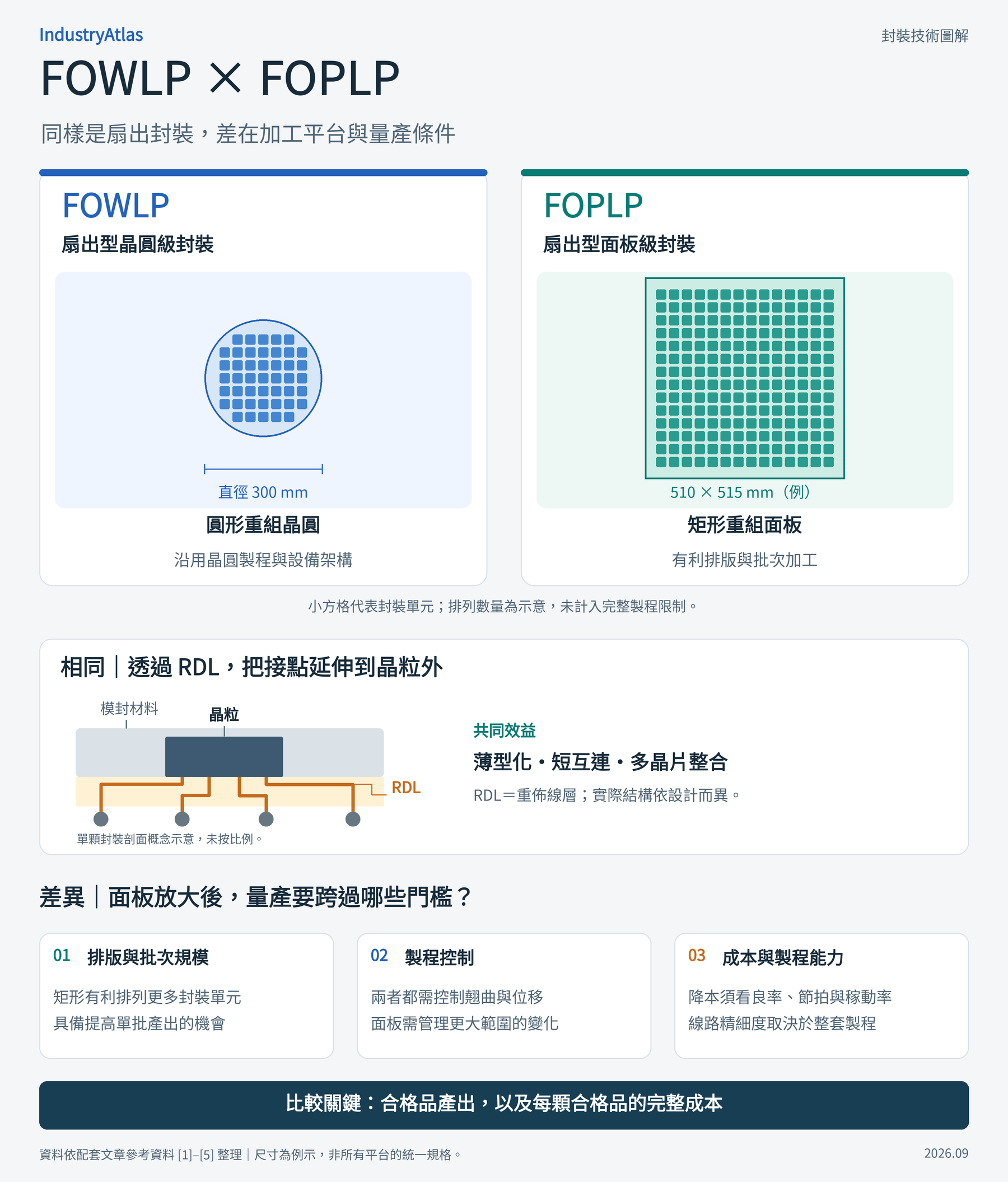
From wafers to panels: the common foundation of fan-out packaging
Fan-out wafer-level packaging (FOWLP) and fan-out panel-level packaging (FOPLP) both use redistribution layers (RDLs) to extend a chip's electrical connections outward, allowing package contacts beyond the die's footprint. [1]
This architecture can enable thinner packages, shorter interconnect paths, and integration of multiple chips. These benefits come from the fan-out structure and are available on either manufacturing platform. [1]
The most visible difference is the processing format: FOWLP uses a circular wafer format, while FOPLP uses rectangular panels. In a common chip-first flow, dies are diced, rearranged, and molded before the RDL is fabricated. FOWLP may therefore process a reconstituted wafer; it should not be understood as completing every packaging step on the original silicon wafer. [1]
Technical comparison
| Comparison | FOWLP | FOPLP |
|---|---|---|
| Processing format | Circular reconstituted wafer | Rectangular reconstituted panel |
| Example dimensions | 300 mm diameter | 510 × 515 mm or 600 × 600 mm; dimensions vary by platform |
| Layout characteristics | Rectangular packages leave unusable portions near the circular edge | Rectangular layouts can reduce edge-area losses |
| Film formation | Can use spin coating familiar from wafer processing | Can use dry-film lamination, slot-die coating, and other methods matched to materials and equipment |
| Process-control priorities | Die shift, warpage, registration, and film uniformity | The same issues, plus dimensional variation across a larger area |
| Fine-line capability | Depends on imaging, materials, metallization, and registration | Also depends on the complete process; panel shape does not determine linewidth |
| Cost-assessment priorities | Batch cost, output, yield, and equipment utilization | Whether larger batches offset equipment costs, processing time, and yield losses |
This is a general comparison of manufacturing platforms. Actual specifications depend on the packaging provider's process conditions. [2][3][4][5]
FOPLP's main opportunity: larger batches and better layouts
Panel processing offers the direct opportunity to arrange more packages across a larger processing area. A 510 × 515 mm panel has approximately 3.7 times the geometric area of a 300 mm-diameter wafer. That is a dimensional calculation before edge exclusions, saw streets, and other process restrictions are deducted. [2]
Rectangular panels also lend themselves to rectangular package layouts. As packages grow, the number of rows and columns and the losses near the edges directly affect usable output. Package dimensions and panel dimensions therefore need to be optimized together. [5]
A larger area does not automatically increase hourly output by the same proportion. Exposure time may rise with the processing area, while operations such as die placement retain a per-die cost. Bottlenecks must be assessed across the entire production line. [2]
What becomes more difficult as panels grow?
FOPLP's engineering challenge is to maintain sufficiently consistent processing quality for packages at different locations across a large area. Warpage, die shift, and fine-line fabrication remain central issues in panel-level packaging research. [4]
First, warpage and dimensional stability. Materials, layer thicknesses, copper distribution, and curing conditions all affect deformation and must be controlled through carrier and process design. [3]
Second, die shift and registration. Die positions can deviate from their intended locations after placement and molding. Finer circuits generally require tighter alignment between contacts and the RDL, making measurement, shift compensation, and adaptive imaging necessary. [3][4]
Third, uniformity of dielectric and metal layers. Thickness and pattern quality must be controlled from dielectric films and photoresist through copper circuitry. Dry film is one option for panel processing, and suppliers have introduced dry-film photoresists for advanced-packaging RDLs. A change in material format still requires validation with imaging and downstream processes. [3][7]
These problems also exist in FOWLP. Comparing the two requires measured results for a specific product and line; processing dimensions alone cannot establish which has the higher yield. [2][4]
Will process capability improve? It depends on the circuitry and architecture
FOPLP can support high-density interconnect development, but moving to panels and making finer traces are separate engineering tasks. Line/space (L/S), RDL layer count, registration accuracy, and reliability must each be verified. [3][4]
Powertech Technology, for example, discloses chip-first and chip-last architectures in its panel-level fan-out portfolio. Its chip-last platform lists a minimum RDL L/S of 2/2 μm. This describes a particular platform's capability, not a universal FOPLP specification or the production yield of every product. [6]
Process sequence also changes the distribution of risk. A flow that fabricates the RDL before attaching dies can screen the circuitry first, reducing the chance of placing expensive dies on defective RDLs. Subsequent bonding and packaging still require yield control. [6]
Electrical and thermal performance must therefore be assessed through interconnect length, materials, package structure, and heat-flow paths. A circular or rectangular processing format cannot by itself determine the finished product's performance. This is an engineering assessment based on package-design conditions. [3]
Is there a cost advantage? Compare the complete cost per good package
Cost comparisons should use the total cost per qualified package and consistently define whether die cost is included. Materials, processing time, equipment, facilities, and yield must all be counted, particularly the loss of dies when a process fails. [5]
A 2024 cost-modeling study considered a 6 × 6 mm package with a single RDL. Under equal-yield and equal-factory-parameter assumptions, it estimated that 515 × 510 mm and 600 × 600 mm panels could reduce cost per package by approximately 42% and 50%, respectively, relative to a 300 mm wafer. The author also noted that overhead on a new production line could reduce the savings. These are model results for a particular scenario, not universal quotations or promised cost reductions. [2]
Yield consequently carries substantial economic weight. Additional metrology or process improvements may increase upfront spending yet reduce total cost if they cut scrap. Scrapping an entire panel may lose more dies, but whether a local defect causes the loss of a whole panel depends on its extent and the process response. [5]
How should a suitable platform be selected?
The technical and cost considerations above suggest three questions:
1. Can it meet the product specification consistently? Compare results at the same package dimensions, RDL layer count, L/S, and reliability requirements.
2. Can it increase good-unit output? Measure qualified packages per hour across the whole line, rather than only the number that fit on a wafer or panel.
3. Can it reduce the complete unit cost? Include equipment utilization, materials, testing, scrap, and die losses using a consistent cost boundary.
A product already manufactured reliably with FOWLP needs sufficient benefit to justify new equipment and qualification for panels. Products with large volumes, efficient layouts, and suitable process conditions can use FOPLP to expand manufacturing scale. The choice should ultimately follow product requirements and verifiable production data.
Sources & notes
- [1] Fraunhofer IZM, Fan-out Wafer- Panel Level Packaging.
- https://www.izm.fraunhofer.de/en/abteilungen/system_integrationinterconnectiontechnologies/arbeitsgebiete/fan-out-wafer-level-packaging.html
- [2] Amy Lujan / SavanSys Solutions LLC, Panel-level Fan-out: Relationship Between Panel Size and Cost Reduction, IMAPS 2024 Symposium, 2024.
- https://imapsource.org/article/129618.pdf
- [3] BroadPak, Fan-Out and Panel-Level Packaging.
- https://www.broadpak.com/fan-out-panel-level-packaging.html
- [4] Fraunhofer IZM, Panel Level Packaging Consortium.
- https://www.izm.fraunhofer.de/en/institut/netzwerk_weltweit/panel-level-consortium-2-0.html
- [5] Fraunhofer IZM / RealIZM, The Advantages of Cost Modelling in Packaging Processes, August 20, 2020.
- https://blog.izm.fraunhofer.de/the-advantages-of-cost-modelling-in-packaging-processes/
- [6] Powertech Technology Inc., Panel Level Fan Out.
- https://www.pti.com.tw/en/tech/advancetechnologycategories/panel-level-fan-out
- [7] Asahi Kasei, Asahi Kasei launches new series of Sunfort™ dry film photoresist as material for back-end processing of advanced semiconductor packaging used in AI servers, May 26, 2025.
- https://www.asahi-kasei.com/news/2025/e250526
- Sources accessed September 28, 2026.