
INDUSTRY ANALYSIS
HBM4 and HBM4E Technology and Supply Chains: How the Three Major Suppliers Combine Memory Processes and Advanced Packaging
Competition in HBM4 and HBM4E spans DRAM dies, logic base dies, and stacked packaging. SK hynix, Samsung, and Micron use different process combinations, creating distinct roles for foundries, bonding-equipment makers, packaging-material suppliers, test providers, and substrate manufacturers. Understanding this supply chain starts with separating product generations, manufacturing technologies, and publicly confirmed partnerships.
What is HBM4E? Product generations and process generations are different
As AI accelerators become faster, memory must deliver data quickly enough to keep them supplied. High-bandwidth memory (HBM) vertically stacks DRAM dies, transfers signals through through-silicon vias (TSVs) and inter-die contacts, and connects to GPUs or other accelerators through high-density packaging. [1][16]
HBM4E is the enhanced generation following HBM4. Micron's HBM4E and SK hynix's or Samsung's HBM4 are not different names for products of the same generation. All three suppliers have their own HBM4 and subsequent HBM4E roadmaps. [3][4][6][9]
A product upgrade does not require every manufacturing stage to change technology simultaneously. HBM process analysis should distinguish at least three parts:
1. DRAM dies: store data. Their process and design affect capacity density, power consumption, and yield.
2. Logic base die: sits beneath the stack and handles interface and control functions. It is also becoming an important location for customization.
3. Stacking and packaging: bonds the dies and addresses electrical connections, thickness, cooling, and structural reliability.
“1c DRAM,” “4 nm base die,” and “MR-MUF” therefore describe three different dimensions. They cannot be compared along one process-node scale.
Principal differences between HBM4 and HBM4E
An important change from HBM3E to HBM4 is the expansion of the external data interface from 1,024 bits to 2,048 bits. HBM4E builds on that architecture with higher transfer rates, capacity, and energy efficiency, while expanding customization options. [1][13]
| Comparison | HBM4 | HBM4E | Manufacturing and supply-chain implications |
|---|---|---|---|
| Product positioning | New generation following HBM3E | Enhanced generation following HBM4 | Sampling, qualification, and production progress must be tracked separately |
| Data-interface width | 2,048 bits | Publicly disclosed interface solutions retain 2,048 bits | Bandwidth gains depend more on per-pin speed and interface design |
| Disclosed speed examples | Micron: above 11 Gbps; Samsung: 11.7 Gbps, with higher-speed capability also disclosed | Samsung samples: stable operation at 14 Gbps and up to 16 Gbps; SK hynix samples: up to 16 Gbps | More demanding signal integrity, power delivery, cooling, and testing |
| Capacity examples | 12-high 36GB; 16-high 48GB products or samples also exist | SK hynix and Samsung have announced 12-high 48GB samples | Higher density per DRAM die can increase capacity without only adding layers |
| DRAM process | Different nodes across suppliers | Some change nodes; others retain a node and improve the design | There is no single HBM4E process recipe shared by all three |
| Logic base die | Memory suppliers already cooperate with logic foundries | Standard and customized products coexist | Foundries, interface IP, and co-design become more important |
| Die bonding | Continued improvement of established microbump and stacking technologies | Established technologies extend further, alongside evaluation or selective introduction of hybrid bonding | HBM4E does not imply a universal switch to hybrid bonding |
Sources: [1][4][5][6][7][8][13][25]. Speeds and capacities are supplier examples, not guaranteed specifications shared by every product. A sample's maximum speed is not necessarily its operating speed in a customer's system.
For a 2,048-bit interface operating at 12 Gbps per data pin, theoretical bandwidth is 2,048 × 12 ÷ 8 = 3,072 GB/s, or approximately 3.07 TB/s. This is an interface calculation; real applications also depend on the controller, access patterns, and system design.
Comparing the three suppliers' HBM4 and HBM4E processes
The differences center on when DRAM processes advance, who manufactures the base die, and how established packaging capabilities are extended.
| Supplier/product | DRAM die process | Logic base die and manufacturing responsibilities | Public progress and evidence limits |
|---|---|---|---|
| SK hynix HBM4 | 1b, fifth-generation 10 nm-class DRAM | TSMC cooperation using its advanced logic processes for the base die | Volume shipments announced; official cooperation information does not limit every version to one foundry node. [1][2] |
| SK hynix HBM4E | Official newsroom technical interview discusses a 1c direction | Specific base-die nodes have not been fully disclosed | 12-high 48GB samples shipped. The 1c information is a public technical direction and must be distinguished from final product specifications. [3][4] |
| Samsung HBM4 | 1c, sixth-generation 10 nm-class DRAM | Samsung Foundry 4 nm base die | Commercial volume shipments announced in February 2026. [5] |
| Samsung HBM4E | Announced samples retain 1c | Announced samples retain Samsung Foundry 4 nm base dies | Sampling announced in May 2026; design and process optimization improve performance. [6] |
| Micron HBM4 | 1β (1-beta) | Base die and DRAM dies designed and manufactured internally | High-volume shipments in 2026, including 12-high 36GB products. [7][8][9] |
| Micron HBM4E | 1γ (1-gamma) | TSMC cooperation for standard and customized base dies | Public plan targets calendar 2027 production. Detailed foundry nodes are not fully disclosed in the primary sources cited here. [8][9] |
Process names need separate interpretation. 1b, 1c, 1β, and 1γ are suppliers' DRAM technology-generation names, not “1 nanometer.” Names from different companies cannot be directly converted into identical physical dimensions. The base die's 4 nm label is a logic-process designation, a different basis of comparison from a DRAM node.
SK hynix: DRAM, logic foundry, and MR-MUF advance together
SK hynix's HBM4 uses 1b DRAM and a logic base die developed with TSMC. HBM manufacturing therefore involves both memory processing and logic foundry work. The partners also cooperate on HBM integration with CoWoS. [1][2]
SK hynix's announced 12-high 48GB HBM4E samples continue to use Advanced MR-MUF. This demonstrates that higher capacity and speed can accompany continued improvement of an established stacking technology. [4]
Samsung: upgrading through design optimization while retaining 1c and 4 nm
Samsung combines DRAM, logic foundry, and packaging capabilities. Both its HBM4 and announced HBM4E samples use 1c DRAM and 4 nm base dies. [5][6]
Samsung HBM4E therefore cannot be summarized as “requiring 1d DRAM or a 2 nm base die.” Upgrades in the public samples include memory and logic architecture optimization, higher capacity, and improvements in low-power and packaging design. Later customized versions should be assessed through their individual announcements. [6]
Micron: from internal base-die manufacturing to cooperation with TSMC
Micron's HBM4 uses 1β DRAM and internally designed and manufactured base dies. HBM4E moves to 1γ DRAM and cooperation with TSMC on standard and customized base dies. Among the three suppliers, this represents a particularly clear change in manufacturing responsibilities. [8][9]
Changes in 1γ include EUV lithography and a new generation of high-k metal-gate technology. Process evolution therefore includes both patterning and transistor technology. Improvements reported for general DRAM cannot, however, be directly treated as HBM4E finished-product performance or yield gains. [11]
In its September 2026 earnings materials, Micron disclosed work with NVIDIA on NVHBM, a customized HBM4E implementation intended for later GPU and NVLink Fusion platforms. This is public progress in customization, not evidence that all HBM4E uses the same design. [10]
How stacking works: MR-MUF, TC-NCF, and hybrid bonding
“12-high” or “16-high” usually counts the DRAM dies; a base die sits underneath. Thinner dies and taller stacks increase the importance of bonding precision, warpage control, thermal management, and yield.
| Technology | How the process works | Principal engineering issues | Public relationship to HBM4/HBM4E |
|---|---|---|---|
| MR-MUF: mass reflow and molded underfill | Position and stack dies, reflow the microbump joints, then fill and protect the gaps with molding material | Fill uniformity, voids, warpage, cooling, and process efficiency | SK hynix explicitly identifies Advanced MR-MUF for HBM4 and HBM4E. [1][4][14] |
| TC-NCF: thermocompression bonding and non-conductive film | Heat and pressure bond the dies; NCF provides filling, insulation, and structural protection. Current still passes through metal contacts | Alignment, pressure and temperature control, film properties, and bonding time | Samsung says it has 16-high TC-NCF production-technology capability; this does not mean every 16-high product is already in production. [12] |
| Hybrid bonding | Directly bond dielectric layers and copper contacts, eliminating conventional solder microbumps at that interface | Surface planarity, cleanliness, copper-surface preparation, and alignment | Samsung has supplied hybrid-copper-bonded HBM4 samples and plans partial commercialization at the HBM4E stage. [12][16] |
HBM4E does not require every supplier to adopt hybrid bonding throughout. SK hynix's HBM4E samples retain MR-MUF. Samsung's hybrid copper bonding must be distinguished between sampling and commercialization plans. Micron's detailed HBM4/HBM4E bonding flows are not fully disclosed in the primary sources used here; a definitive equipment and materials list should not be filled in by assumption.
The comparison also should not be reduced to whether a process “uses adhesive.” MR-MUF and TC-NCF materials primarily provide protection, insulation, and mechanical support. Hybrid bonding changes the die-bonding interface; it does not imply that the entire package no longer needs polymers.
Process supply chain: who does what?
The HBM supply chain spans product design and wafer fabrication, TSV processing and stacking, and testing and system packaging. The following distinguishes confirmed products or partnerships, confirmed HBM-related business, and technical capability alone. Relevant capability does not establish an HBM4 or HBM4E order from a particular memory supplier.
Design, DRAM, and logic base dies
| Process/stage | Representative companies | Work and publicly disclosed relationships |
|---|---|---|
| DRAM design, fabrication, and HBM product integration | SK hynix, Samsung, Micron | All three offer HBM4 and are advancing HBM4E, with their own DRAM technologies, product designs, and stack integration. [1][4][5][6][7][9] |
| Base-die wafer fabrication | TSMC, Samsung Foundry, Micron | TSMC cooperates with SK hynix on HBM4 and Micron on HBM4E. Samsung's announced HBM4/4E base dies use its own 4 nm process. Micron manufactures HBM4 base dies internally. [2][5][6][8] |
| HBM interface IP, controllers, and ASIC design support | Global Unichip (GUC), Synopsys, Cadence | GUC has demonstrated 12 Gbps HBM4 PHY/controller IP on TSMC 3 nm. Synopsys and Cadence offer HBM4/HBM4E-related interface IP. [13][15] |
GUC's 3 nm HBM4 IP demonstration does not establish that a memory supplier's base die uses 3 nm. The HBM controller/PHY on the accelerator side and the base die underneath the memory stack are different design locations. GUC's announcement confirms an IP platform and packaging demonstration, not that it designed a base die for a named HBM manufacturer. [15]
Lithography, TSVs, thinning, bonding equipment, and materials
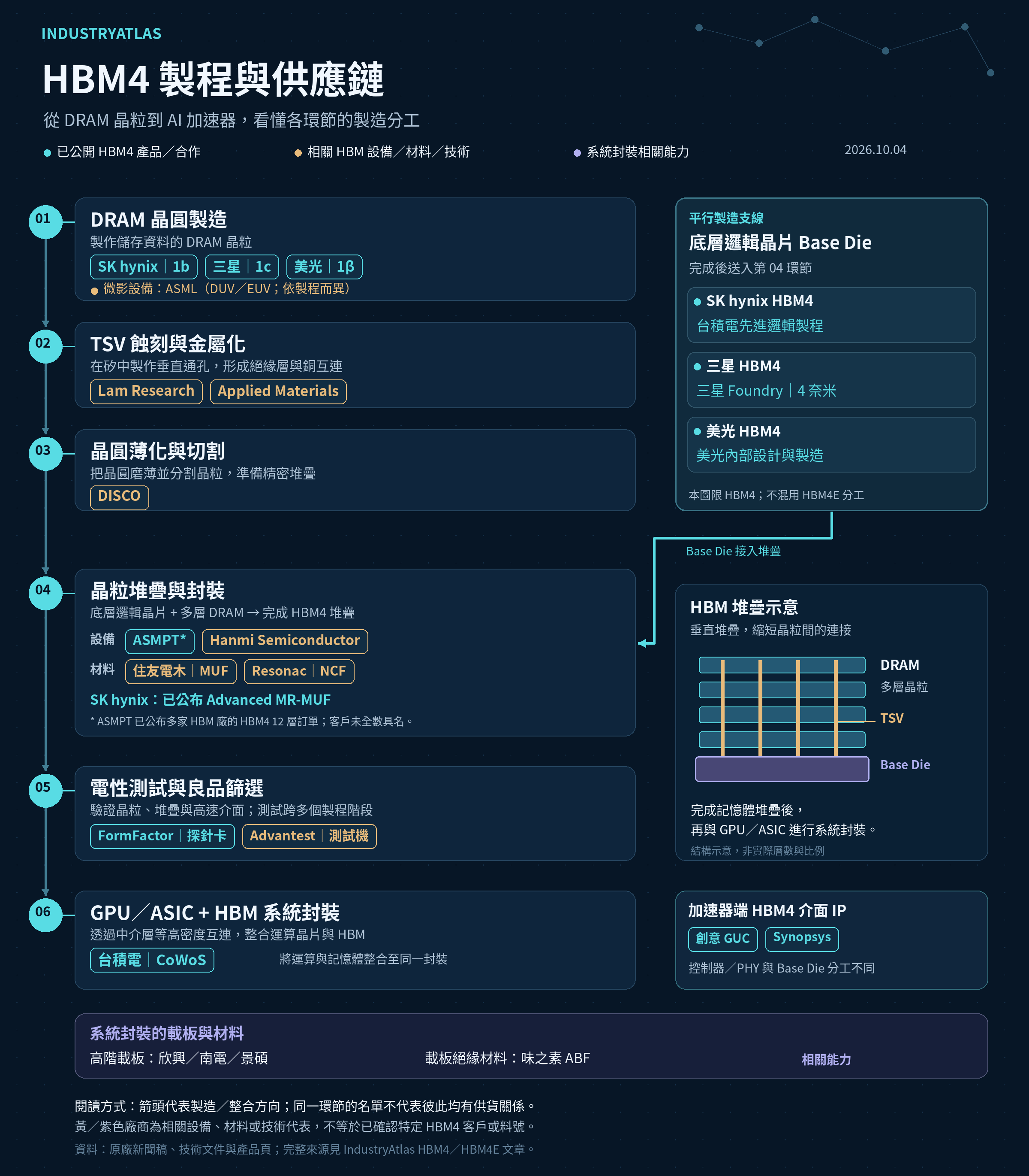
| Process/stage | Representative companies | Participation | Limits of public evidence |
|---|---|---|---|
| DRAM and logic lithography | ASML | DUV/EUV systems supporting advanced DRAM and logic processes | Equipment and application areas are confirmed; not every HBM4/4E process layer should be assumed to use EUV. [26] |
| TSV etching, films, and metallization | Lam Research, Applied Materials | Vertical holes, insulating/barrier layers, and copper interconnects; Lam discloses HBM-related solutions including Syndion and SABRE 3D | HBM/TSV process capabilities are confirmed; equipment configurations are not fully public for every supplier and generation. [16] |
| Wafer thinning and dicing | DISCO | Grinding, thinning, and cutting to enable thin-die processing and stacking | Official technical materials identify HBM applications, but do not establish exclusive supply to a specific manufacturer. [17] |
| Precision stacking and thermocompression bonding equipment | Hanmi Semiconductor, ASMPT | Equipment for HBM die stacking/bonding | Hanmi publicly displays HBM TC BONDERS. ASMPT explicitly reports HBM4 12-high orders from multiple HBM manufacturers without naming every customer. [18][19] |
| Molding and underfill materials | Sumitomo Bakelite | HBM packaging materials, including MUF-related products | HBM material products are confirmed; supply for every HBM4/4E model is not. [20] |
| Non-conductive film (NCF) | Resonac | Insulating, filling, and bonding material for die stacking | HBM NCF and expansion plans are public; particular HBM4/4E customers and material grades require separate confirmation. [20] |
Bonding equipment and packaging materials need joint process tuning. The name “TC Bonder” alone does not establish that an entire line uses TC-NCF. Its actual role—placement, pre-bonding, or final bonding—must be identified.
Testing, system packaging, and substrates
| Process/stage | Representative companies | Participation and evidence limits |
|---|---|---|
| Wafer and HBM electrical testing | Advantest, FormFactor | Advantest supplies memory testers; FormFactor discloses HBM4 probe-card solutions. Testing screens good dies and verifies high-speed interfaces, but complete supplier configurations are not public. [21] |
| High-density GPU/ASIC and HBM packaging | TSMC | CoWoS integrates compute chips with HBM; SK hynix and TSMC have disclosed related cooperation. [2] |
| Heterogeneous integration and memory-stacking services | ASE, Powertech Technology (PTI) | ASE VIPack supports logic/HBM integration. PTI discloses TSV, memory stacking, and thermocompression-bonding capabilities. They are listed as relevant technology/service providers, not as confirmed recipients of specific HBM4/4E production orders. [22] |
| Advanced package substrates | Unimicron, Nan Ya PCB, Kinsus | Advanced IC substrates or FC-BGA products support and electrically connect accelerator packages. Public capability is not confirmation of supply to a specific HBM4/4E project. [23] |
| Substrate insulating materials | Ajinomoto | ABF provides build-up insulation in package substrates. Its location and function differ from MUF/NCF between DRAM dies. [23] |
HBM stacking and CoWoS: two packaging stages with different responsibilities
A common source of confusion is the distinction between making an HBM product and integrating HBM into an AI accelerator package.
The first stage combines DRAM dies, TSVs, and a base die into an HBM stack. It involves die thinning, bonding, underfill, and memory testing.
The second integrates finished HBM with a GPU/ASIC through an interposer or other high-density interconnect structure and connects that assembly to a package substrate. CoWoS belongs to this level of integration. ABF substrates also serve this larger package structure. [2][16][23]
TSMC can consequently have two roles in the same supply chain: base-die foundry manufacturing and advanced accelerator packaging. These are different jobs. Substrate suppliers, assembly/test providers, and HBM manufacturers must likewise be identified by their separate business positions.
How do downstream customers influence HBM technology choices?
HBM specifications and production schedules generally require joint development and qualification with accelerator platforms. Customers consider power, cooling, usable capacity, package space, and stable supply alongside maximum bandwidth.
Specific public examples exist: Micron announced HBM4 for NVIDIA Vera Rubin; SK hynix displayed Rubin-related products with its HBM4; and Samsung's memorandum of understanding with AMD covers cooperation toward a primary HBM4 supply role for AMD Instinct MI455X. [7][24][25]
These link products to platforms, but demonstrations, memoranda of understanding, completed qualification, and high-volume shipments represent different stages. They cannot be used interchangeably. Micron's NVHBM disclosure also shows customized HBM4E deepening cooperation between memory suppliers and accelerator designers. [10]
Sources & notes
- Primarily supplier releases, technical documents, earnings materials, and official product pages. Information cutoff: October 4, 2026. Roadmaps and production plans retain their forward-looking status.
- [1] SK hynix: HBM4 development completion and preparation for mass production, September 12, 2025; Q2 2026 business results, July 29, 2026.
- https://news.skhynix.com/en/sk-hynix-completes-worlds-first-hbm4-development-and-readies-mass-production/
- https://news.skhynix.com/en/q2-2026-business-results/
- [2] SK hynix: Cooperation with TSMC to advance HBM technology, April 19, 2024.
- https://news.skhynix.com/en/sk-hynix-partners-with-tsmc-to-strengthen-hbm-technological-leadership/
- [3] SK hynix: Future Talents Class, HBM, TSVs, MR-MUF, and future technologies, June 8, 2026. Expert technical interview published in the official newsroom.
- https://news.skhynix.co.kr/future-talents-class-ep1/
- [4] SK hynix: Shipment of 12-high HBM4E samples, June 18, 2026.
- https://news.skhynix.com/en/sk-hynix-ships-samples-of-12-layer-next-gen-hbm4e-2/
- [5] Samsung: HBM4 commercial shipments and process specifications, February 12, 2026.
- https://news.samsung.com/global/samsung-ships-industry-first-commercial-hbm4-with-ultimate-performance-for-ai-computing
- [6] Samsung: HBM4E sample shipments and process specifications, May 29, 2026.
- https://news.samsung.com/global/samsung-electronics-begins-shipment-of-industry-first-hbm4e-samples
- [7] Micron: HBM4 sampling announcement, June 10, 2025; HBM4 production for NVIDIA Vera Rubin, March 16, 2026.
- https://investors.micron.com/news/press-release/2025/Micron-Ships-HBM4-to-Key-Customers-to-Power-Next-Gen-AI-Platforms-06-10-2025/default.aspx
- https://investors.micron.com/news/press-release/2026/Micron-in-High-Volume-Production-of-HBM4-Designed-for-NVIDIA-Vera-Rubin-PCIe-Gen6-SSD-and-SOCAMM2-03-16-2026/default.aspx
- [8] Micron: Quarterly results archive; FY2025 Q4 Prepared Remarks, September 23, 2025, on HBM4E/TSMC cooperation; FY2026 Q1 Prepared Remarks, December 17, 2025, on internal HBM4 design and manufacturing.
- https://investors.micron.com/financials/quarterly-results/default.aspx
- [9] Micron: FY2026 Q3 earnings release, SEC filing, June 24, 2026. HBM4 1β, HBM4E 1γ, and production plans.
- https://www.sec.gov/Archives/edgar/data/723125/000072312526000013/a2026q3ex991-pressrelease.htm
- [10] Micron: FY2026 Q4 Prepared Remarks, September 30, 2026. NVHBM cooperation.
- https://s25.q4cdn.com/621799436/files/doc_financials/2026/q4/Q4-FY26-Prepared-Remarks.pdf
- [11] Micron: 1γ DRAM technology.
- https://www.micron.com/products/memory/1gamma-dram-technology
- [12] Samsung: Q4 2025 earnings-call transcript, Korean, pp. 25–26. TC-NCF and hybrid copper bonding.
- https://irsvc.teletogether.com/sec/pdf/2025Q4_script_kor.pdf?1=
- [13] Cadence: HBM4E PHY; Synopsys: HBM4 PHY.
- https://www.cadence.com/en_US/home/tools/silicon-solutions/design-ip/memory-interface-and-storage-ip/hbm-phy/hbm4e.html
- https://www.synopsys.com/designware-ip/interface-ip/hbm/hbm4-phy.html
- [14] SK hynix: MR-MUF technology and thermal management, July 30, 2024.
- https://news.skhynix.com/en/rulebreaker-revolutions-mr-muf-unlocks-hbm-heat-control/
- [15] Global Unichip: 3 nm, 12 Gbps HBM4 PHY/controller demonstration, April 23, 2026.
- https://www.guc-asic.com/en/news/all/PR_20260423
- [16] Lam Research: High-Bandwidth Memory Explained, September 11, 2025; Applied Materials: TSV process solutions.
- https://newsroom.lamresearch.com/high-bandwidth-memory-explained-semi-101
- https://www.appliedmaterials.com/us/en/semiconductor/markets-and-inflections/heterogeneous-integration/tsv.html
- [17] DISCO: Technical Briefing 2023. HBM wafer thinning and processing.
- https://www-hq.disco.co.jp/jp/ir/movie/doc/E_Tech_Briefing_2023.pdf
- [18] ASMPT: TCB technology and HBM4 12-high orders, February 5, 2026.
- https://www.asmpt.com/en/investor-relations/news-events/asmpt-extends-technology-leadership-with-key-tcb-aor-chip-to-wafer-milestone/
- [19] Hanmi Semiconductor: TC BONDER 4 product page in the official COMPUTEX exhibitor directory; KRX investor-meeting announcement, July 16, 2026.
- https://www.computextaipei.com.tw/zh-tw/product/CBA4659B8C39B7F764E0B08D1538393F39AB6D47E55E4F6F/info.html
- https://kind.krx.co.kr/corpgeneral/irschedule.do?irSeq=45162&method=searchIRScheduleDetail
- [20] Sumitomo Bakelite: Semiconductor-related materials business; Resonac: AI chip material expansion and HBM NCF, March 29, 2024.
- https://www.sumibe.co.jp/ir/segment/semiconductor/
- https://eu.resonac.com/2903_24/
- [21] Advantest: July 2025 earnings Q&A; FormFactor: High-speed known-good-die wafer testing for memory ICs, 2025.
- https://www.advantest.com/document/en/investors/ir-library/result/E_BIZ_250729_QA.pdf
- https://www.formfactor.com/blog/2025/high-speed-test-solutions-for-known-good-die-wafer-test-on-memory-ics/
- [22] ASE: VIPack platform; PTI: TSV Solution.
- https://ase.aseglobal.com/VIPack/
- https://www.pti.com.tw/en/tech/advancetechnologycategories/tsv-solution
- [23] Unimicron: Products and sustainable innovation; Nan Ya Plastics: Business overview and introduction to Nan Ya PCB; Kinsus: Product overview; Ajinomoto: Electronic-material technologies and ABF.
- https://www.uniflex.com.tw/esg/en/product01.html
- https://www.npc.com.tw/j2npc/zhtw/company_highlights.jsp
- https://www.kinsus.com.tw/zh-tw/product/products/products_overview
- https://www.ajinomoto.com/innovation/rd-organizations-and-facilities/bioscience_chemicals/technology
- [24] Samsung: Expanded next-generation AI memory cooperation with AMD, March 18, 2026.
- https://news.samsung.com/global/samsung-and-amd-expand-strategic-collaboration-on-next-generation-ai-memory-solutions
- [25] SK hynix: Memory products at TSMC OIP Conference 2026, September 28, 2026.
- https://news.skhynix.com/en/tsmc-oip-conference-2026/
- [26] ASML: EUV lithography systems; Company and DUV/EUV technology introduction.
- https://www.asml.com/en/products/euv-lithography-systems
- https://www.asml.com/en/company/about-asml