
INDUSTRY ANALYSIS
Why Glass Core Substrates Are Attracting NVIDIA's Attention: From Material Advantages to Manufacturing
Progress in AI chips is extending beyond scaling individual transistors toward packaging multiple dies and high-bandwidth memory together. Flatness, dimensional stability, and adjustable thermal expansion make glass core substrates an important candidate for next-generation large packages. Recent media reports of NVIDIA encouraging their development point to requirements for computing power, memory bandwidth, and production readiness. This article examines glass-core advantages, NVIDIA's possible engineering considerations, and the process from glass selection and through-glass vias to metallization, circuit fabrication, and inspection.
As AI chips become more powerful, packaging must keep pace
A high-performance AI accelerator is no longer simply one compute chip. Multiple dies, high-bandwidth memory (HBM), and numerous power and signal connections must work together in limited space. Packaging must accommodate larger areas, denser circuitry, and thermomechanical stresses during manufacturing and operation. [1][3]
The glass core substrate (GCS) discussed here replaces the organic composite core of an IC package substrate with glass. The glass remains permanently in the finished product. Together with metallized vias, insulating build-up layers, and copper circuits, it connects the chip package to the system circuit board. [3][10][11]
This differs from a temporary glass carrier removed after processing. It is also not automatically equivalent to a glass interposer that provides fine interconnections between chips. The core, build-up circuitry, interposer, and system PCB occupy different levels. Adopting a glass core does not mean the other structures disappear.
Glass combines dimensional stability with precision
Organic substrates continue to improve. Resonac, for example, has used materials simulation to improve low-thermal-expansion CCL and address warpage and cracking in large packages. Interest in glass should therefore be understood as a response to increasingly demanding combinations of properties, rather than evidence that all organic materials have exhausted their potential. [15]
Flatness and dimensional stability in large packages
As package area grows, local deformation, thickness variation, and interlayer displacement become harder to control. These affect imaging registration, fine-line fabrication, and chip bonding, not merely appearance. Glass-core rigidity and dimensional stability offer a way to reduce warpage in larger packages. [2][3]
In its 2023 disclosure, Intel said its glass approach could reduce pattern distortion by approximately 50% relative to the organic substrates used for comparison, with the potential for a tenfold increase in interconnect density. These are comparisons for a particular technology. They do not mean every glass substrate achieves ten times the density, and cannot be translated into ten times the GPU performance. [1]
Adjustable thermal expansion
A package combines silicon, copper, insulating materials, and a core. These expand by different amounts when heated and may retain stress after cooling. Glass composition can be adjusted to tune its coefficient of thermal expansion (CTE), providing more options for matching the overall package. [2]
For example, a low-loss glass under development at SCHOTT lists a CTE of approximately 3.29 ppm/K. A lower value is not automatically better: compatibility with copper vias, build-up materials, solder joints, and the board must also be considered. Reducing deformation in one location can shift stress to another interface. [4][15]
Denser electrical connections and more integration options
Metallized through-glass vias (TGVs) connect circuitry on the two sides of the core. Combined with fine redistribution layers (RDLs), glass cores may support denser signal and power connections. [3][10]
Longer-term possibilities include photonic/electronic integration. Corning has proposed combining optical waveguides and electrical redistribution in future glass cores for co-packaged optics. This remains a further integration direction. Transparent glass does not perform electrical-to-optical conversion on its own, and not every glass core contains optical waveguides. [2]
Electrical and thermal performance require separate assessments
Glass electrical properties depend on its formulation; glass cannot be assumed superior to every advanced CCL. The SCHOTT material cited above has published values of approximately Dk 4.05 and Df 0.0021 at 10 GHz. These are not universal glass-core specifications, and should not be ranked against M9/M10 without considering measurement methods and circuit structures. [4]
Heat resistance and thermal conductivity are also different properties. Maintaining dimensional stability during processing does not mean glass rapidly removes heat from a GPU. SCHOTT's technical information lists room-temperature thermal conductivities of approximately 0.5–1.38 W/(m·K) for various glasses. Overall heat removal still depends on metallic thermal paths and cooling-system design. [13]
Why might NVIDIA want suppliers to prepare sooner?
On September 24, 2026, the Seoul Economic Daily reported that Jensen Huang had discussed next-generation semiconductor cooperation, including glass substrates, with SK Group Chairman Chey Tae-won, and was encouraging TSMC to develop related technology. [6]
The evidentiary boundary matters: this is a media report. This article has not obtained a full transcript of Huang publicly asking for glass-substrate development to accelerate, and the report does not confirm adoption by a specific GPU. The following explanations are technical analysis based on public product and materials developments.
First, multidie integration is already a real product direction. NVIDIA describes Blackwell Ultra as two nearly reticle-limit dies linked by a 10 TB/s die-to-die interface. This shows that GPU expansion depends on coordinated operation within the package; it does not mean Blackwell Ultra already uses a glass core. [5]
Second, additional computing power needs memory and connectivity to match. More compute units and transistors may deliver limited benefit if usable memory bandwidth and data movement cannot increase. As an engineering inference, materials enabling larger packages and denser interconnects create room for future die and HBM arrangements. The extent of that expansion still depends on interposers, controllers, power delivery, and cooling.
Finally, product design and manufacturing capability must be aligned in advance. DNP's plan disclosed at the end of 2025 called for samples from a new pilot line in early 2026, with a full volume-production system targeted for FY2028. Sampling, reliability evaluation, and stable supply require a substantial preparation period. [3]
If NVIDIA wants glass cores available for future products, it is reasonable to encourage joint development of materials, equipment, and substrate processes early. The urgency can be understood as preparation for next-generation packaging capability, rather than imminent elimination of existing substrates.
How a sheet of glass becomes a usable package substrate

Manufacturing a glass core substrate involves three broad tasks: form precise structures in the glass, establish metal conduction, and build multilayer circuits with verified reliability.
The illustrative flow below uses a glass core with metallized TGVs and build-up layers on both sides. Suppliers vary the materials, via-formation methods, and sequence, and some stages repeat. This is not any company's fixed production recipe.
| Stage | Main work | Result |
|---|---|---|
| 1 Material selection and preparation | Select glass composition, thickness, and dimensions; verify flatness and surface/edge quality; remove contamination | A glass core suitable for precision processing |
| 2 TGV formation | Create through-holes according to the design, for example by laser modification followed by selective etching | Glass vias that are not yet conductive |
| 3 Via inspection and cleaning | Check diameter, shape, location, and defects; remove residues | Via walls suitable for metallization |
| 4 Adhesion treatment and seed layer | Improve glass-to-metal bonding and form a thin, continuous conductive layer | Surfaces and via walls that can be electroplated |
| 5 TGV metallization | Fill vias with copper or form sufficiently thick metal on their walls; planarize if required | Conductive paths between the two glass surfaces |
| 6 Insulating build-up and via opening | Apply insulation and open microvias where connections are required | An insulating structure supporting the next circuit layer |
| 7 RDL fabrication | Pattern and deposit metal to create fine traces; repeat build-up as designed | Multilayer circuits routing dense contacts to their intended locations |
| 8 Outer contacts and protection | Form external contacts; apply surface finishes and open protective layers to suit the bonding method | Interfaces for chip-package or board connections |
| 9 Singulation and visual inspection | Separate the processing unit into individual substrates while controlling chipping, cracks, and contamination | Individual substrates meeting dimensional requirements |
| 10 Electrical and reliability testing | Check continuity and insulation; evaluate reliability using samples or test structures | Quality data for customer qualification and subsequent assembly decisions |
This flow combines public information from via-formation, metallization, substrate, and inspection suppliers. Quality checks take place throughout, not only at the end. Chip assembly and final package testing are subsequent parts of the process. [7]–[12]
Forming a hole and making it conductive are different operations
LPKF's LIDE technology, for example, first uses an ultrafast laser to modify selected regions inside glass. Selective wet etching then removes those regions to form through-holes. This differs from directly ablating all the glass with a laser. [7]
After holes are formed, metal adhesion still needs to be addressed. Glass is insulating, and its surface chemistry makes reliable metallization challenging. A wet-process route announced by Atotech in 2026 first establishes a metal-oxide adhesion layer, then forms a continuous electroless-copper seed layer, followed by pulse-plated via filling. [8]
The seed layer provides the conductive foundation for electroplating; it is not a completed via fill. Continuity of coverage, voids in the copper, and interface quality all affect reliable operation. Some TGV designs metallize the walls rather than creating solid copper columns. [3][8]
RDLs turn vias into a complete circuit
TGVs provide vertical connections, while RDLs route signals laterally and distribute contacts. A sheet of drilled, copper-filled glass alone cannot provide all the connections needed by a complex package. [10]
In a typical semi-additive process (SAP), a thin conductive layer is formed first. Photoresist exposure and development define the traces, electroplating thickens the required copper, and the resist and excess seed layer are removed. Insulating build-up layers and microvias allow circuitry to be built layer by layer; the exact sequence depends on process integration. [9]
Glass cores therefore do not eliminate all resins and insulating films. Structures under development already include ABF build-up layers. Inspection equipment must also detect internal glass cracks after metallization and ABF processing. [11]
The hardest production challenge is preventing defects from accumulating
Glass rigidity helps preserve shape, but brittleness makes edge chipping, microcracks, and interface damage important risks. Defects that are initially small can grow during later processing. Singulation methods must consequently be evaluated against the full material stack and its protection measures. [10][12]
Inspection must also look inside the structure. In September 2026, Spirox disclosed TGV crack-inspection equipment and related technical exchanges, reflecting supply-chain work on quality control after metallization and build-up processing. [11]
Manufacturing capability means more than successfully drilling or plating once. Large glass panels must retain quality through multiple operations and meet customers' electrical and reliability requirements consistently. This explains the continuing investment needed between promising material properties and widespread use in AI packaging.
How glass cores and advanced CCL can coexist
Glass cores primarily change the core of a package substrate. M9/M10-grade CCL largely addresses high-speed signals at board level. Panasonic, for example, positions MEGTRON9 for high-speed circuit-board designs supporting 224 Gbps. The technologies occupy different levels: a glass-core package can still be mounted on a PCB made with advanced CCL. [3][16]
If more interconnects move into the package or become optical, demand for some high-speed PCB traces may change. That would be an effect of architectural evolution, not a reason to assume an immediate downgrade of board materials merely because the package core becomes glass.
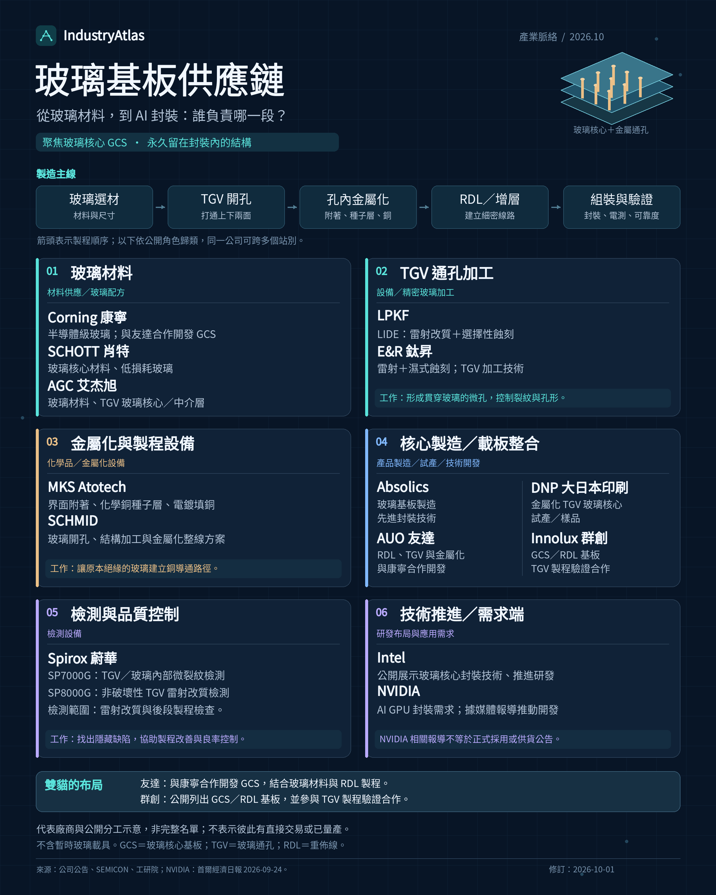
Progress to watch includes full package qualification, control of process defects, and whether scale improves cost. AUO and Corning's publicly demonstrated 2026 cooperation brings glass materials, RDLs, TGV metallization, and reliability verification onto the same development path. Materials, manufacturing, and system design must mature together for these advantages to reach next-generation AI products. [14]
Sources & notes
- Numbered references correspond to the text. Except for item 6, a media report, these are original company technical materials, announcements, or research papers. Undated material refers to content accessible on September 30, 2026. Source descriptions are retained from the Chinese article; no missing URLs have been inferred.
- [1] Intel, Intel Unveils Industry-Leading Glass Substrates to Meet Demand for More Powerful Compute, September 18, 2023. Dimensional stability, interconnect density, and positioning.
- [2] Corning, Co-packaged optics: The future of data centers. Glass-core thermomechanical properties, adjustable CTE, and future photonic/electronic integration.
- [3] DNP, DNP to Launch New TGV Glass core Substrate Pilot Line at Kuki Plant, December 16, 2025. Substrate position, TGV structures, and pilot/volume-production planning.
- [4] SCHOTT, Technical Details of SCHOTT low-loss. CTE, Dk, Df, and test frequency for a material under development.
- [5] NVIDIA, Inside NVIDIA Blackwell Ultra: The Chip Powering the AI Factory Era. Dual-die design and 10 TB/s die-to-die interface.
- [6] Seoul Economic Daily, Nvidia Weighs Glass Substrates to Stack More HBM on AI Chips, September 24, 2026. Media reporting on Huang's discussions and encouragement of development. The English page translates a Korean report; it is not a verbatim quotation or formal adoption commitment.
- [7] LPKF, LIDE Technology: Industry Standard for Advanced Glass Processing. Two-stage laser modification and selective wet etching.
- [8] MKS Atotech, MKS' Atotech introduces integrated wet metallization process for glass substrates, July 28, 2026. Adhesion promotion, electroless-copper seed layers, and pulse via filling.
- [9] Merschky, M. et al., Using a Metal Oxide Adhesion Layer and Wet Chemical Cu Metallization for Fine Line Pattern Formation on Glass, 2017, IMAPSource Proceedings, pp. 458–463. Glass metallization and SAP pattern formation. DOI reference in the original source list.
- [10] LPKF, Glass Core Substrates: TGV Formation & Panel-Level Processing. TGVs, RDLs, panel processing, and crack risks.
- [11] Spirox, Spirox Launches High-Speed TGV Crack Inspection System to Support High-Volume Glass Substrate Inspection, September 8, 2026. Internal microcrack detection after metallization and ABF build-up.
- [12] DISCO, Cutting Process Using Laser. Laser ablation, stealth dicing, and contamination control.
- [13] SCHOTT, Technical Information. Glass heat-transfer properties and room-temperature thermal-conductivity range. Original PDF.
- [14] AUO, AUO Showcases Micro LED Optical Communication and Glass Core Substrates Technologies at SEMICON Taiwan 2026, August 31, 2026. AUO/Corning glass-core, RDL, and process development.
- [15] Resonac, Resonac Develops Low Thermal Expansion Copper-Clad Laminates for Next-Generation Semiconductor Packages through Simulation, 2025. Low-CTE organic cores and trade-offs between warpage and cracking.
- [16] Panasonic, Panasonic Industry Electronic Materials is enabling the 224 Gbps revolution with Megtron 9!, January 15, 2025. High-speed board-material application positioning.